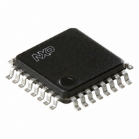
TDA8020HL/C2,118 NXP Semiconductors, TDA8020HL/C2,118 Datasheet - Page 9

TDA8020HL/C2,118
Manufacturer Part Number
TDA8020HL/C2,118
Description
IC SMART CARD INTERFACE 32LQFP
Manufacturer
NXP Semiconductors
Type
Interfacer
Datasheet
1.TDA8020HLC2118.pdf
(28 pages)
Specifications of TDA8020HL/C2,118
Package / Case
32-LQFP
Voltage - Supply
2.7 V ~ 6.5 V
Mounting Type
Surface Mount
Maximum Operating Temperature
+ 85 C
Minimum Operating Temperature
- 40 C
Mounting Style
SMD/SMT
Lead Free Status / RoHS Status
Lead free / RoHS Compliant
Number Of Drivers/receivers
-
Protocol
-
Lead Free Status / Rohs Status
Lead free / RoHS Compliant
Other names
568-3522-2
935272983118
TDA8020HL2BD-T
935272983118
TDA8020HL2BD-T
Available stocks
Company
Part Number
Manufacturer
Quantity
Price
Company:
Part Number:
TDA8020HL/C2,118
Manufacturer:
NXP Semiconductors
Quantity:
10 000
Part Number:
TDA8020HL/C2,118
Manufacturer:
NXP/恩智浦
Quantity:
20 000
Philips Semiconductors
called the master. The devices that are controlled by the
master are called slaves.
Each byte is followed by one HIGH-level acknowledge bit
asserted by the transmitter. The master generates an
extra acknowledge related clock pulse. The slave receiver
which is addressed is obliged to generate an acknowledge
after the reception of each byte.
The master receiver must generate an acknowledge after
the reception of each byte that has been clocked out of the
slave transmitter.
The device that acknowledges has to pull-down the SDA
line during the acknowledge clock pulse in such a way that
the SDA line is stable LOW during the HIGH period of the
acknowledge related clock pulse.
Set-up and hold times must be taken into account.
A master receiver must signal an end of data to the slave
Table 1 Proposed device address bit allocations
Table 2 Proposed I
2003 Nov 06
TDA8020HL
Dual IC card interface
Device
PIN SAD1
HIGH
HIGH
LOW
LOW
2
7
0
C-bus addresses for 4 devices in parallel
6
1
PIN SAD0
HIGH
HIGH
LOW
LOW
5
0
9
4
0
Address bits
transmitter by not generating an acknowledge on the last
byte that has been clocked out of the slave. In this event,
the transmitter must leave the data line HIGH to enable the
master generation of the STOP condition.
See Chapter “Characteristics” for timing information.
D
Each device has 2 different addresses, one for each card.
An application can use up to four devices in parallel by the
use of address selection pins SAD0 and SAD1.
Pins SAD0 and SAD1 are externally hardwired to V
GND; SAD0 specifies address bit A0, SAD1 specifies
address bit A1; Address bit R/W specifies either read or
write operation: logic 1 = Read, logic 0 = Write (see
Tables 1 and 2).
EVICE ADDRESSING
CARD 1
0/1
40H
42H
44H
46H
3
A1
2
TDA8020HL
Product specification
A0
1
CARD 2
4AH
4CH
4EH
48H
R/W
0
DD
or


