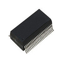
ICS1893BFI IDT, Integrated Device Technology Inc, ICS1893BFI Datasheet - Page 24

ICS1893BFI
Manufacturer Part Number
ICS1893BFI
Description
PHYCEIVER LOW PWR 3.3V 48-SSOP
Manufacturer
IDT, Integrated Device Technology Inc
Series
PHYceiver™r
Type
PHY Transceiverr
Specifications of ICS1893BFI
Protocol
MII
Voltage - Supply
3.14 V ~ 3.47 V
Mounting Type
Surface Mount
Package / Case
48-SSOP
Lead Free Status / RoHS Status
Contains lead / RoHS non-compliant
Number Of Drivers/receivers
-
Lead Free Status / Rohs Status
Not Compliant
Other names
1893BFI
Available stocks
Company
Part Number
Manufacturer
Quantity
Price
Company:
Part Number:
ICS1893BFI
Manufacturer:
OKI
Quantity:
1 934
Part Number:
ICS1893BFILF
Manufacturer:
ICS
Quantity:
20 000
5.1 MII Data Interface
ICS1893BF, Rev. F, 5/13/10
The ICS1893BF’s MAC Interface is the Media Independent Interface (MII) operating at either 10 Mbps or
100 Mbps. The ICS1893BF MAC Interface is configured for the MII Data Interface mode, data is transferred
between the PHY and the MAC as framed, 4-bit parallel nibbles. In addition, the interface also provides
status and control signals to synchronize the transfers.
The ICS1893BF provides a full complement of the ISO/IEC-specified MII signals. Its MII has both a transmit
and a receive data path to synchronously exchange 4 bits of data (that is, nibbles).
•
•
Both the MII transmit clock and the MII receive clock are provided to the MAC/Reconciliation sublayer by
the ICS1893BF (that is, the ICS1893BF sources the TXCLK and RXCLK signals to the MAC).
Clause 22 also defines as part of the MII a Carrier Sense signal (CRS) and a Collision Detect signal (COL).
The ICS1893BF is fully compliant with these definitions and sources both of these signals to the MAC.
When operating in:
•
•
As mentioned in
is, it is possible to connect its MII to a MAC when power is already applied to the MAC. To support this
functionality, the ICS1893BF isolates its MII signals and tri-states the signals on all Twisted-Pair Transmit
pins (TP_TXP and TP_TXN) during a power-on reset. Upon completion of the reset process, the
ICS1893BF enables its MII and enables its Twisted-Pair Transmit signals.
The ICS1893BF’s MII transmit data path includes the following:
The ICS1893BF’s MII receive data path includes the following:
Half-duplex mode, the ICS1893BF asserts the Carrier Sense signal when data is being either transmitted
or received. While operating in half-duplex mode, the ICS1893BF also asserts its Collision Detect signal
to indicate that data is being received while a transmission is in progress.
Full-duplex mode, the ICS1893BF asserts the Carrier Sense signal only when receiving data and forces
the Collision Detect signal to remain inactive.
– A data nibble, TXD[3:0]
– A transmit data clock to synchronize transfers, TXCLK
– A transmit enable signal, TXEN
– The TXER pin is not available on the ICS1893BF
– A separate data nibble, RXD[3:0]
– A receive data clock to synchronize transfers, RXCLK
– A receive data valid signal, RXDV
ICS1893BF Data Sheet - Release
Section 4.1.1.3, “Hot
Insertion”, the ICS1893BF design allows hot insertion of its MII. That
Copyright © 2009, IDT, Inc.
All rights reserved.
24
Chapter 5 Interface Overviews
May, 2010


