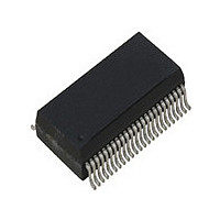
ICS1893BFI IDT, Integrated Device Technology Inc, ICS1893BFI Datasheet - Page 28

ICS1893BFI
Manufacturer Part Number
ICS1893BFI
Description
PHYCEIVER LOW PWR 3.3V 48-SSOP
Manufacturer
IDT, Integrated Device Technology Inc
Series
PHYceiver™r
Type
PHY Transceiverr
Specifications of ICS1893BFI
Protocol
MII
Voltage - Supply
3.14 V ~ 3.47 V
Mounting Type
Surface Mount
Package / Case
48-SSOP
Lead Free Status / RoHS Status
Contains lead / RoHS non-compliant
Number Of Drivers/receivers
-
Lead Free Status / Rohs Status
Not Compliant
Other names
1893BFI
Available stocks
Company
Part Number
Manufacturer
Quantity
Price
Company:
Part Number:
ICS1893BFI
Manufacturer:
OKI
Quantity:
1 934
Part Number:
ICS1893BFILF
Manufacturer:
ICS
Quantity:
20 000
ICS1893BF, Rev. F, 5/13/10
If a crystal is used as the clocking source, connect it to both the Ref_in (pin 47) and Ref_out (pin 46) pins
of the ICS1893BF. A pair of bypass capacitors on either side of the crystal are connected to ground. The
crystal is used in the parallel resonance or anti-resonance mode. The value of the bypass caps serve to
adjust the final frequency of the crystal oscillation. Typical applications would use 33pF bypass caps. The
exact value will be affected by the board routing capacitance on Ref_in and Ref_out pins. Smaller bypass
capacitors raise the frequency of oscillation. Once the exact value of bypass capacitance is established it
will be the same for all boards using the same specification crystal. The best way to measure the crystal
frequency is to measure the frequency of TXCLK (pin 37) using a frequency counter with a 10 second
sample. Using TXCLK prevents affecting the crystal frequency by the measurement. The crystal
specification is shown in Table 5.1.
Table 5-1. 25MHz Crystal Specification
Table 5-2. 25MHz Oscillator Specification
Specifications
Fundamental Frequency
(tolerance is sum of freq.,
temp., stability and aging.)
Freq. Tolerance
Input Capacitance
Specifications
Output Frequency
Freq. Stability (including aging)
Duty cycle CMOS level
one-half VDD
VIH
VIL
Period Jitter
Input Capacitance
ICS1893BF Data Sheet - Release
Symbol Minimum
F0
∆
Cin
Symbol Minimum
F0
∆
Tw/T
Tjitter
CIN
F/f
F/f
Copyright © 2009, IDT, Inc.
All rights reserved.
24.99875 25.00000
24.99875 25.00000
28
2.79
35
Typical Maximum
Typical Maximum
3
3
25.00125
25.00125
±
±
0.33
500
50
50
65
Chapter 5 Interface Overviews
Volts
Volts
MHz
MHz
Unit
ppm
Unit
ppm
pS
pF
pF
%
May, 2010


