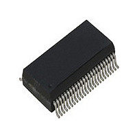
ICS1893BFI IDT, Integrated Device Technology Inc, ICS1893BFI Datasheet - Page 51

ICS1893BFI
Manufacturer Part Number
ICS1893BFI
Description
PHYCEIVER LOW PWR 3.3V 48-SSOP
Manufacturer
IDT, Integrated Device Technology Inc
Series
PHYceiver™r
Type
PHY Transceiverr
Specifications of ICS1893BFI
Protocol
MII
Voltage - Supply
3.14 V ~ 3.47 V
Mounting Type
Surface Mount
Package / Case
48-SSOP
Lead Free Status / RoHS Status
Contains lead / RoHS non-compliant
Number Of Drivers/receivers
-
Lead Free Status / Rohs Status
Not Compliant
Other names
1893BFI
Available stocks
Company
Part Number
Manufacturer
Quantity
Price
Company:
Part Number:
ICS1893BFI
Manufacturer:
OKI
Quantity:
1 934
Part Number:
ICS1893BFILF
Manufacturer:
ICS
Quantity:
20 000
7.1.2 Management Register Bit Access
7.1.3 Management Register Bit Default Values
ICS1893BF, Rev. F, 5/13/10
The ICS1893BF Management Registers include one or more of the following types of bits:
Table 7-3. Description of Management Register Bit Types
The tables in this chapter specify for each register bit the default value, if one exists. The ICS1893BF sets
all Management Register bits to their default values after a reset.
ICS1893BF Management Register bits.
Table 7-4. Range of Possible Valid Default Values for ICS1893BF Register Bits
Note:
Read-Only
Command Override
Write
Read/Write
Read/Write Zero
Register Bit Types
State of pin at reset
Default Condition
Management
ICS1893BF Data Sheet Rev. F - Release
The ICS1893BF has a number of reserved bits throughout the Management Registers. Most of
these bits provide enhanced test modes. The Management Register tables provide the default
values for these bits. The STA must not change the value of these bits under any circumstance. If
the STA inadvertently changes the default values of these reserved register bits, normal operation
of the ICS1893BF can be affected.
–
0
1
Indicates there is no default value for the bit
Indicates the bit’s default value is logic zero
Indicates the bit’s default value is logic one
For some bits, the default value depends on the state (that is, the logic value) of a
particular pin at reset (that is, the logic value of a pin is latched at reset). An
example of pins that have a default condition that depends on the state of the pin
at reset are the PHY / LED pins (P0AC, P1CL, P2LI, P3TD, and P4RD) discussed
in the following sections:
Symbol
•
•
•
R/W0
R/W
CW
RO
Bit
Section 5.5, “Status Interface”
Section 7.11, “Register 16: Extended Control Register”
Section 8.2.2, “Multi-Function (Multiplexed) Pins: PHY Address and LED Pins”
An STA can obtain the value of a RO register bit. However, it cannot
alter the value of (that is, it cannot write to) an RO register bit. The
ICS1893BF isolates any STA attempt to write a value to an RO bit.
An STA can read a value from a CW register bit. However, write
operations are conditional, based on the value of the Command
Register Override bit (bit 16.15). When bit 16.15 is logic:
An STA can unconditionally read from or write to a R/W register bit.
An STA can unconditionally read from a R/W0 register bit, but only a
‘0’ value can be written to this bit.
•
•
Zero (the default), the ICS1893BF isolates STA attempts to write to
the CW bits (that is, CW bits cannot be altered when bit 16.15 is
logic zero).
One, the ICS1893BF permits an STA to alter the value of the CW
bits in the subsequent register write. (Bit 16.15 is self-clearing and
automatically clears to zero on the subsequent write.)
Copyright © 2009, IDT, Inc.
All rights reserved.
51
Default Value
Description
Table 7-4
Chapter 7 Management Register Set
lists the valid default values for
May, 2010


