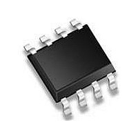
UC3845BD STMicroelectronics, UC3845BD Datasheet - Page 2

UC3845BD
Manufacturer Part Number
UC3845BD
Description
Switching Converters, Regulators & Controllers 0.5mA Current Mode
Manufacturer
STMicroelectronics
Datasheet
1.UC3844BD.pdf
(15 pages)
Specifications of UC3845BD
Output Voltage
4.90 V to 5.10 V
Switching Frequency
52 kHz
Operating Temperature Range
- 40 C to + 150 C
Mounting Style
SMD/SMT
Package / Case
SO-8
Duty Cycle (max)
50 %
Lead Free Status / Rohs Status
Lead free / RoHS Compliant
Available stocks
Company
Part Number
Manufacturer
Quantity
Price
Company:
Part Number:
UC3845BD1
Manufacturer:
ST
Quantity:
18 420
Company:
Part Number:
UC3845BD1013TR
Manufacturer:
STM
Quantity:
12 500
Part Number:
UC3845BD1013TR
Manufacturer:
ST
Quantity:
20 000
Company:
Part Number:
UC3845BD1G
Manufacturer:
ON Semiconductor
Quantity:
2 000
Part Number:
UC3845BD1R2G
Manufacturer:
ON/安森美
Quantity:
20 000
* All voltages are with respect to pin 5, all currents are positive into the specified terminal.
UC2842B/3B/4B/5B - UC3842B/3B/4B/5B
ABSOLUTE MAXIMUM RATINGS
PIN CONNECTION (top view)
PIN FUNCTIONS
ORDERING NUMBERS
2/15
Symbol
No
1
2
3
4
5
6
7
8
T
P
P
E
T
T
V
V
I
O
stg
tot
tot
O
J
L
i
i
GROUND
Function
OUTPUT
COMP
I
R
SENSE
V
V
V
T
Supply Voltage (low impedance source)
Supply Voltage (Ii < 30mA)
Output Current
Output Energy (capacitive load)
Analog Inputs (pins 2, 3)
Error Amplifier Output Sink Current
Power Dissipation at T
Power Dissipation at Tamb
Storage Temperature Range
Junction Operating Temperature
Lead Temperature (soldering 10s)
CC
/C
FB
ref
UC2842BD1; UC3842BD1
UC2843BD1; UC3843BD1
UC2844BD1; UC3844BD1
UC2845BD1; UC3845BD1
T
This pin is the Error Amplifier output and is made available for loop compensation.
This is the inverting input of the Error Amplifier. It is normally connected to the switching
power supply output through a resistor divider.
A voltage proportional to inductor current is connected to this input. The PWM uses this
information to terminate the output switch conduction.
The oscillator frequency and maximum Output duty cycle are programmed by connecting
resistor R
This pin is the combined control circuitry and power ground.
This output directly drives the gate of a power MOSFET. Peak currents up to 1A are sourced
and sunk by this pin.
This pin is the positive supply of the control IC.
This is the reference output. It provides charging current for capacitor C
SO8
T
to Vref and cpacitor C
amb
COMP
I
R
SENSE
T
V
/C
Parameter
FB
T
25 C (Minidip)
25 C (SO8)
1
2
3
4
Minidip/SO8
D95IN332
T
to ground. Operation to 500kHz is possible.
8
7
6
5
Description
V
Vi
OUTPUT
GROUND
REF
UC2842BN; UC3842BN
UC2843BN; UC3843BN
UC2844BN; UC3844BN
UC2845BN; UC3845BN
Minidip
Self Limiting
– 0.3 to 5.5
– 65 to 150
– 40 to 150
Value
1.25
800
300
30
10
5
1
T
through resistor R
Unit
mW
mA
°C
W
V
A
V
C
C
J
T
.


