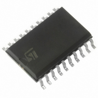
L6221CD013TR STMicroelectronics, L6221CD013TR Datasheet

L6221CD013TR
Specifications of L6221CD013TR
Available stocks
Related parts for L6221CD013TR
L6221CD013TR Summary of contents
Page 1
FOUR NON INVERTING INPUTS WITH . ENABLE . OUTPUT VOLTAGE OUTPUT CURRENT VERY LOW SATURATION VOLTAGE . TTL COMPATIBLE INPUTS INTEGRAL FAST RECIRCULATION DIODES DESCRIPTION The L6221 monolithic ...
Page 2
L6221C THERMAL DATA Symbol R Thermal Resistance Junction-pins th j-pins R Thermal Resistance Junction-case th j-case R Thermal Resistance Junction-ambient th j-amb PIN CONNECTIONS (top views) L6221C (Powerdip) 2/15 Parameter Max. Max. Max. OUT4 CLAMPB N.C. OUT3 GND GND OUT2 ...
Page 3
ABSOLUTE MAXIMUM RATINGS Symbol V Output Voltage O V Logic Supply Voltage Input Voltage, Enable Voltage Continuous Colllector Current (for each channel Collector Peak Current (repetitive, duty cycle = 10% ton ...
Page 4
L6221C ELECTRICAL CHARACTERISTICS Refer to The Test Circuit to Fig.1 to Fig.9 (V otherwise specified) Symbol Parameter V Logic Supply Voltage S I Logic Supply Current S I Output Leakage Current CEX V Collector Emitter Saturation Voltage CE(sat) (one input ...
Page 5
TEST CIRCUITS (X) = Referred to Multiwatt package X = Referred to Powerdip package Figure 1 : Logic supply current 4.5V 0.8V 0.8V 2V, ...
Page 6
L6221C Figure 4 : Collector-emitter Saturation Voltage. Figure 6 : Clamp Diode Leakage Current +60V P 6/15 Figure 5 : Logic Input Characteristics open 0.8V for ...
Page 7
Figure 8 : Switching Times Test Circuit. Figure 10 : Allowed Peak Collector Cur- rent vs. Duty Cycle for Contemporary Working Outputs (L6221C). Figure 9 : Switching TImes Waveforms. Figure 11 : Allowed Peak Collector ...
Page 8
L6221C Figure 12 : Collector Saturation Voltage vs. Collector Current. Figure 14 : Collector Saturation Voltage vs. Junction Temperature 1A. C Figure 16 : Saturation Voltage vs. Junc- tion Temperature 1.8A. 8/15 Figure 13 ...
Page 9
Figure 18. Figure 19 : Driver for Solenoids up to 3A. Some care must be taken to ensure that the collec- tors are placed close together to avoid different cur- rent partitioning at turn-off. We suggest to put in parallel ...
Page 10
L6221C Figure 20 : Saturation Voltage vs. Collector Current. Figure 22 : Peak Collector Current vs. Duty Cycle for Paralleled Outputs Driven (L6221CN). 10/15 Figure 21 : Peak Collector Current vs. Duty Cycle for ...
Page 11
MOUNTING INSTRUCTION The R of the L6221C can be reduced by sol- th j-amb dering the GND pins to a suitable copper area of the printed circuit board (Fig. 23 external heatsink (Fig. 24). The diagram of ...
Page 12
L6221C mm DIM. MIN. TYP. MAX. MIN 2. 0.49 0.55 0.019 F 0.66 0.75 0.026 G 1.02 1.27 1.52 0.040 G1 17.53 17.78 18.03 0.690 H1 19.6 0.772 H2 20.2 L 21.9 ...
Page 13
DIM. MIN. TYP. MAX. MIN. a1 0.51 0.020 B 0.85 1.40 0.033 b 0.50 b1 0.38 0.50 0.015 D 20.0 E 8.80 e 2.54 e3 17.78 F 7.10 I 5.10 L 3.30 Z 1.27 inch MECHANICAL DATA TYP. MAX. ...
Page 14
L6221C mm DIM. MIN. TYP. MAX. MIN. A 2.35 2.65 0.093 A1 0.1 0.3 0.004 B 0.33 0.51 0.013 C 0.23 0.32 0.009 D 12.6 13 0.496 E 7.4 7.6 0.291 e 1. 10.65 0.394 h 0.25 0.75 ...
Page 15
... No license is granted by implication or otherwise under any patent or patent rights of STMicroelectronics. Specification mentioned in this publication are subject to change without notice. This publication supersedes and replaces all information previously supplied. STMi- croelectronics products are not authorized for use as critical components in life support devices or systems without express written approval of STMicroelectronics ...


