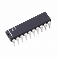
LTC1060CN Linear Technology, LTC1060CN Datasheet - Page 15

LTC1060CN
Manufacturer Part Number
LTC1060CN
Description
IC FILTER BUILDING BLOCK 20-DIP
Manufacturer
Linear Technology
Datasheet
1.LTC1060CNPBF.pdf
(20 pages)
Specifications of LTC1060CN
Filter Type
Universal Switched Capacitor
Frequency - Cutoff Or Center
30kHz
Number Of Filters
2
Max-order
4th
Voltage - Supply
±2.37 V ~ 5 V
Mounting Type
Through Hole
Package / Case
20-DIP (0.300", 7.62mm)
Lead Free Status / RoHS Status
Contains lead / RoHS non-compliant
Available stocks
Company
Part Number
Manufacturer
Quantity
Price
W
There are basically three modes of operation: mode 1,
mode 2, mode 3. In the mode 1 (Figure 4), the input
amplifier is outside the resonant loop. Because of this,
mode 1 and its derivatives (mode 1a, 1b, 1c) are faster
than modes 2 and 3. In mode 1, for instance, the Q errors
are becoming noticeable above 1MHz clock frequency.
Mode 1a (Figure 5), represents the most simple hook-up
of the LTC1060. Mode 1a is useful when voltage gain at the
bandpass output is required. The bandpass voltage gain,
however, is equal to the value of Q; if this is acceptable,
a second order, clock tunable, BP resonator can be achiev-
ed with only 2 resistors. The filter center frequency directly
depends on the external clock frequency. For high order
filters, mode 1a is not practical since it may require several
clock frequencies to tune the overall filter response.
Mode 1 (Figure 4), provides a clock tunable notch; the
depth is shown in Graph 14. Mode 1 is a practical
configuration for second order clock tunable bandpass/
notch filters. In mode 1, a bandpass output with a very
high Q, together with unity gain, can be obtained without
creating problems with the dynamics of the
remaining notch and lowpass outputs.
Modes 1b and 1c (Figures 6 and 7), are similar. They both
produce a notch with a frequency which is always equal to
the filter building block center frequency. The notch and
the center frequency, however, can be adjusted with an
external resistor ratio.
COMM
Figure 17. Mode 6b: 1st Order Filter Providing Lowpass
ODES OF OPERATIO
W W
S
V
A/B
6
–
(17)
15
4
E TS
U
–
+
R3
R2
f
C
=
100(50) R3
f
CLK
ON
R2
3
; H
U
LP1
(18)
+
1/2 LTC1060
OLP1
V
5
THE
IN
= 1 ; H
–
–
S1A
(16)
OLP2
= –
M
2
W
TLC1060 • MOO14
R3
R2
LP2
(19)
U
ODES OF OPERATIO
1
(20)
The practical clock-to-center frequency ratio range is:
The input impedance of the S1 pin is clock dependent,
and in general R5 should not be larger than 5k. Mode 1b
can be used to increase the clock-to-center frequency
ratio beyond 100:1. For this mode, a practical limit for the
(f
large output offsets. Mode 1c is the fastest mode of
operation: In the 50:1 mode and with (R5 = 0, R6 = ∞) the
clock-to-center frequency ratio becomes (50/√2) and cen-
ter frequencies beyond 20kHz can easily be achieved as
shown in Graph 25. Figure 19 illustrates how to cascade
the two sections of the LTC1060 connected in mode 1c to
obtain a sharp fourth order, 1dB ripple, BP Chebyshev
filter. Note that the center frequency to the BW ratio for this
fourth order bandpass filter is 20/1. By varying the clock
frequency to sweep the filter, the center frequency of the
overall filter will increase proportionally and so will the BW
to maintain the 20:1 ratio constant. All the modes of
operation yield constant Q’s; with any filter realization the
BW’s will vary when the filter is swept. This is shown in
Figure 19, where the BP filter is swept from 1kHz to 20kHz
center frequency.
Figure 18. Mode 7: 1st Order Filter Providing Allpass, Lowpass
CLK
500
100
V
1
1
IN
/f
0
) ratio is 500:1. Beyond this, the filter will exhibit
≥
or
R1=R2
S
V
f
A/B
6
f
–
P
CLK
f 0
50
=
1
100(50) R3
U
(17)
15
f
4
CLK
≥
≥
R2
100
–
+
f
R2=R1
CLK
1
f o
; f
R3
z
=
100(50) R3
≥
f
or
CLK
100
√2
R2
50
3
1
AP
(18)
+
; GAIN AT AP OUTPUT = 1 FOR 0 f
1/2 LTC1060
or
; mode 1b
5
–
–
S1A
(16)
50
√2
; mode 1c
2
H
TLC1060 • MOO15
OLP
LP
(19)
LTC1060
= 2 x
1
R3
R2
(20)
f
CLK
2
15
1060fb


