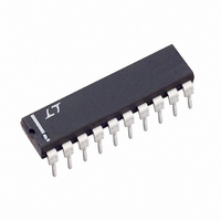
LTC1060CN Linear Technology, LTC1060CN Datasheet - Page 9

LTC1060CN
Manufacturer Part Number
LTC1060CN
Description
IC FILTER BUILDING BLOCK 20-DIP
Manufacturer
Linear Technology
Datasheet
1.LTC1060CNPBF.pdf
(20 pages)
Specifications of LTC1060CN
Filter Type
Universal Switched Capacitor
Frequency - Cutoff Or Center
30kHz
Number Of Filters
2
Max-order
4th
Voltage - Supply
±2.37 V ~ 5 V
Mounting Type
Through Hole
Package / Case
20-DIP (0.300", 7.62mm)
Lead Free Status / RoHS Status
Contains lead / RoHS non-compliant
Available stocks
Company
Part Number
Manufacturer
Quantity
Price
APPLICATIO S I FOR ATIO
Table 2. Wideband RMS Noise
Short-Circuit Currents
Short circuits to ground, positive or negative power supply
are allowed as long as the power supplies do not exceed
±5V and the ambient temperature stays below 85˚C.
Above ±5V and at elevated temperatures, continuous
Each building block of the LTC1060, together with an
external clock and a few resistors, closely approximates
2nd order filter functions. These are tabulated below in the
frequency domain.
1. Bandpass function: available at the bandpass output
DEFINITION
Pins 2 (19). (Figure 1.)
H
G(s) = H
f
OBP
0
±2.5V
±2.5V
±2.5V
±2.5V
±2.5V
±2.5V
±2.5V
±2.5V
±5V
±5V
±5V
±5V
±5V
±5V
±5V
±5V
U
V
= ω/2π; f
S
pole pair. At this frequency, the phase shift
between input and output is –180˚.
= Gain at ω = ω
OBP
0
U
s
is the center frequency of the complex
2
U
+ (sω
OF FILTER FUNCTIONS
sω
100:1
100:1
100:1
100.1
100:1
100.1
100:1
100:1
50:1
50:1
50:1
50:1
50:1
50:1
50:1
50:1
f
o
U
CLK
f
o
0
o
/Q) + ω
/Q
W
o
2
NOTCH/HP
(µV
U
49 (42)
70 (55)
33 (31)
48 (40)
20 (18)
25 (21)
16 (15)
20 (17)
135
170
100
125
57
72
40
50
RMS
U
)
U
150 (125)
220 (160)
150 (105)
100 (80)
(µV
52 (43)
80 (58)
36 (32)
52 (40)
short circuits to the negative power supply will cause
excessive currents to flow. Under these conditions, the
device will get damaged if the short-circuit current is
allowed to exceed 80mA.
2. Lowpass function: available at the LP output Pins
120
160
115
57
72
40
50
88
BP
RMS
1 (20). (Figure 2.)
H
G(s) = H
)
Q = Quality factor of the complex pole pair. It is the
OLP
ratio of f
der bandpass function. The Q is always mea-
sured at the filter BP output.
DC gain of the LP output.
OLP
186 (155)
240 (180)
150 (119)
106 (87)
(µV
0
75 (65)
90 (88)
48 (43)
66 (55)
s
185
140
100
130
to the –3dB bandwidth of the 2nd or-
2
62
80
42
53
LP
RMS
+ s(ω
)
ω
o
2
o
/Q) + ω
CONDITIONS
Mode1, R1 = R2 = R3
Q = 1
Mode 1, Q = 10
R1 = R3 for BP out
R1 = R2 for LP out
Mode 3, R1 = R2 = R3 = R4
Q = 1
Mode 3, R2 = R4, Q = 10
R3 = R1 for BP out
R4 = R1 for LP and HP out
2
o
LTC1060
1060fb
9


