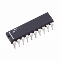
LTC1060CN Linear Technology, LTC1060CN Datasheet - Page 8

LTC1060CN
Manufacturer Part Number
LTC1060CN
Description
IC FILTER BUILDING BLOCK 20-DIP
Manufacturer
Linear Technology
Datasheet
1.LTC1060CNPBF.pdf
(20 pages)
Specifications of LTC1060CN
Filter Type
Universal Switched Capacitor
Frequency - Cutoff Or Center
30kHz
Number Of Filters
2
Max-order
4th
Voltage - Supply
±2.37 V ~ 5 V
Mounting Type
Through Hole
Package / Case
20-DIP (0.300", 7.62mm)
Lead Free Status / RoHS Status
Contains lead / RoHS non-compliant
Available stocks
Company
Part Number
Manufacturer
Quantity
Price
APPLICATIO S I FOR ATIO
internal op amps, as well as the reference point of all the
internal switches are connected to the AGND pin. Because
of this, a “clean” ground is recommended.
f
The f
filter center frequency measured in mode 1, with a Q = 10
and V
500kHz/250kHz for the 100:1/150:1 measurement. All the
curves shown in the Typical Performance Characteristics
section are normalized to the above references.
Graphs 1 and 2 in the Typical Performance Characteristics
show the (f
LTC1060 is a sampled data filter and it only approximates
continuous time filters. In this data sheet, the LTC1060 is
treated in the frequency domain because this approxima-
tion is good enough for most filter applications. The
LTC1060 deviates from its ideal continuous filter model
when the (f
low. Since low Q filters are not selective, the frequency
domain approximation is well justified. In Graph 15 the
LTC1060 is connected in mode 3 and its ( f
adjusted to 200:1 and 500:1. Under these conditions, the
filter is over-sampled and the (f
independent of the Q values. In mode 3, the ( f
typically deviates from the tested one in mode 1 by ±0.1%.
f
This is a figure of merit of general purpose active filter
building blocks. The f
depends on the clock frequency, the power supply volt-
ages, the junction temperature and the mode of operation.
At 25°C ambient temperature for ±5V supplies, and
for clock frequencies below 1MHz, in mode 1 and its
derivatives, the f
desired f
Graph 4 at 50:1 and for f
ideal Q of 400 can be obtained. Under this condition, a
respectable f
16kHz center frequency will be about 0.22% off from the
tested value at 250kHz clock (see Graph 1). For the same
clock frequency of 800kHz and for the same Q value of
400, the f
LTC1060
8
CLK
0
x Q Product Ratio
/f
CLK
0
S
Ratio
= ±5V. The clock frequencies are, respectively,
/f
0
0
0
reference of 100:1 or 50:1 is derived from the
CLK
CLK
x Q product can be further increased if the
0
and Q accuracy. For instance,from
/f
/f
x Q product of 6.4MHz is achieved. The
0
0
) variation versus values of ideal Q. The
0
) ratio decreases and when the Q’s are
x Q product is mainly limited by the
U
0
CLK
U
x Q product of the LTC1060
below 800kHz, a predictable
CLK
W
/f
0
) curves are nearly
CLK
CLK
/f
U
0
/f
) ratio is
0
) ratio
clock-to-center frequency is lowered below 50:1. In mode
1c with R6 = 0 and R6 = ∞, the (f
f
the same clock frequency and same Q value, the filter can
handle a center frequency of 16kHz x √2.
For clock frequencies above 1MHz, the f
limited by the clock frequency itself. From Graph 4 at
±7.5V supply, 50:1 and 1.4MHz clock, a Q of 5 has about
8% error; the measured 28kHz center frequency was
skewed by 0.8% with respect to the guaranteed value at
250kHz clock. Under these conditions, the f
is only 140kHz but the filter can handle higher input signal
frequencies than the 800kHz clock frequency, very high Q
case described above.
Mode 3, Figure 11, and the modes of operation where R4
is finite, are “slower” than the basic mode 1. This is shown
in Graph 16 and 17. The resistor R4 places the input op
amp inside the resonant loop. The finite GBW of this op
amp creates an additional phase shift and enhances the Q
value at high clock frequencies. Graph 16 was drawn with
a small capacitor, C
= ±5V, the (1/2πR4C
2πR4C
curve to be slightly “flatter” over a wider range of clock
frequencies. If, at ±5V supply, the clock is below 900kHz
(or 400kHz for V
For Graph 25, the clock-to-center frequency ratios are
altered to 70.7:1 and 35.35:1. This is done by using mode
1c with R5 = 0, Figure 7, or mode 2 with R2 = R4 = 10kΩ.
The mode 1c, where the input op amp is outside the main
loop, is much faster. Mode 2, however, is more versatile.
At 50:1, and for T
center frequencies up to 30kHz.
Output Noise
The wideband RMS noise of the LTC1060 outputs is nearly
independent from the clock frequency, provided that the
clock itself does not become part of the noise. The LTC1060
noise slightly decreases with ±2.5V supply. The noise at
the BP and LP outputs increases for high Q’s. Table 2
shows typical values of wideband RMS noise. The num-
bers in parentheses are the noise measurement in mode 1
with the S
0
x Q product can now be increased to 9MHz since, with
C
) should be equal to 1.4MHz. This allows the Q
A/B
pin shorted to V
S
= ±2.5V), this capacitor, C
A
C
= 25°C the mode 1c can be tuned for
, placed across R4 and as such, at V
C
) = 2MHz. With V
–
CLK
as shown in Figure 25.
/f
0
) ratio is 50/√2. The
S
0
= ±2.5V the (1/
C
x Q product is
, is not needed.
0
x Q product
1060fb
S


