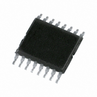
PCA9674PW,112 NXP Semiconductors, PCA9674PW,112 Datasheet - Page 21

PCA9674PW,112
Manufacturer Part Number
PCA9674PW,112
Description
IC I/O EXPANDER I2C 8B 16TSSOP
Manufacturer
NXP Semiconductors
Datasheet
1.PCA9674ABS118.pdf
(32 pages)
Specifications of PCA9674PW,112
Interface
I²C
Number Of I /o
8
Interrupt Output
Yes
Frequency - Clock
1MHz
Voltage - Supply
2.3 V ~ 5.5 V
Operating Temperature
-40°C ~ 85°C
Mounting Type
Surface Mount
Package / Case
16-TSSOP
Includes
POR
Lead Free Status / RoHS Status
Lead free / RoHS Compliant
Other names
935282735112
PCA9674PW
PCA9674PW
PCA9674PW
PCA9674PW
NXP Semiconductors
13. Dynamic characteristics
Table 9.
V
[1]
[2]
[3]
[4]
[5]
[6]
PCA9674_PCA9674A_5
Product data sheet
Symbol Parameter
f
t
t
t
t
t
t
t
t
t
t
t
t
t
Port timing; C
t
t
t
Interrupt timing; C
t
t
SCL
BUF
HD;STA
SU;STA
SU;STO
HD;DAT
VD;ACK
VD;DAT
SU;DAT
LOW
HIGH
f
r
SP
v(Q)
su(D)
h(D)
v(D)
d(rst)
DD
= 2.3 V to 5.5 V; V
t
t
C
A master device must internally provide a hold time of at least 300 ns for the SDA signal (refer to the V
bridge the undefined region SCL’s falling edge.
The maximum t
250 ns. This allows series protection resistors to be connected between the SDA and the SCL pins and the SDA/SCL bus lines without
exceeding the maximum specified t
Input filters on the SDA and SCL inputs suppress noise spikes less than 50 ns.
VD;ACK
VD;DAT
b
= total capacitance of one bus line in pF.
SCL clock frequency
bus free time between a
STOP and START condition
hold time (repeated) START
condition
set-up time for a repeated
START condition
set-up time for STOP
condition
data hold time
data valid acknowledge
time
data valid time
data set-up time
LOW period of the SCL clock
HIGH period of the SCL
clock
fall time of both SDA and
SCL signals
rise time of both SDA and
SCL signals
pulse width of spikes that
must be suppressed by the
input filter
data output valid time
data input set-up time
data input hold time
data input valid time
reset delay time
= minimum time for SDA data out to be valid following SCL LOW.
= time for Acknowledgement signal from SCL LOW to SDA (out) LOW.
Dynamic characteristics
[1]
L
f
100 pF (see
for the SDA and SCL bus lines is specified at 300 ns. The maximum fall time for the SDA output stage t
L
[6]
SS
100 pF (see
[2]
= 0 V; T
Figure 13
amb
f
.
Figure 13
= 40 C to +85 C; unless otherwise specified.
Conditions
and
Figure
and
Rev. 05 — 15 June 2009
Figure
[4][5]
14)
Remote 8-bit I/O expander for Fm+ I
14)
Standard mode
Min
300
250
4.7
4.0
4.7
4.0
0.3
4.7
4.0
0
0
0
4
-
-
-
-
-
-
I
2
C-bus
1000
Max
3.45
100
300
50
4
4
4
-
-
-
-
-
-
-
-
-
-
-
Fast mode I
20 + 0.1C
20 + 0.1C
Min
100
1.3
0.6
0.6
0.6
0.1
1.3
0.6
50
0
0
0
4
-
-
-
-
b
b
[3]
[3]
2
C-bus Fast-mode Plus
PCA9674/74A
Max
400
300
300
0.9
50
4
4
4
-
-
-
-
-
-
-
-
-
-
-
IL
of the SCL signal) in order to
2
C-bus with interrupt
0.26
0.26
0.26
0.05
0.26
Min
0.5
0.5
50
50
0
0
0
4
-
-
-
-
-
-
© NXP B.V. 2009. All rights reserved.
I
2
C-bus
f
1000
Max
0.45
450
120
120
is specified at
50
4
4
4
-
-
-
-
-
-
-
-
-
-
21 of 32
Unit
kHz
ns
ns
ns
ns
ns
ns
s
s
s
s
s
s
s
s
s
s
s
s


