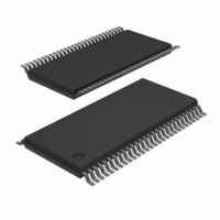
PCA9698DGG,518 NXP Semiconductors, PCA9698DGG,518 Datasheet - Page 15

PCA9698DGG,518
Manufacturer Part Number
PCA9698DGG,518
Description
IC I/O EXPANDER I2C 40B 56TSSOP
Manufacturer
NXP Semiconductors
Datasheet
1.PCA9698BS118.pdf
(48 pages)
Specifications of PCA9698DGG,518
Package / Case
56-TSSOP
Interface
I²C
Number Of I /o
40
Interrupt Output
Yes
Frequency - Clock
1MHz
Voltage - Supply
2.3 V ~ 5.5 V
Operating Temperature
-40°C ~ 85°C
Mounting Type
Surface Mount
Includes
POR
Logic Family
PCA9698
Number Of Lines (input / Output)
40.0 / 40.0
Operating Supply Voltage
2.3 V to 5.5 V
Power Dissipation
500 mW
Operating Temperature Range
- 40 C to + 85 C
Input Voltage
5.5 V
Logic Type
I2C Bus
Maximum Clock Frequency
1 MHz
Mounting Style
SMD/SMT
Number Of Input Lines
40.0
Number Of Output Lines
40.0
Output Current
50 mA
Output Voltage
5.5 V
Lead Free Status / RoHS Status
Lead free / RoHS Compliant
For Use With
OM6281 - DAUGHTER CARD PCA9698 FOR OM6275
Lead Free Status / Rohs Status
Lead free / RoHS Compliant
Other names
935278614518
PCA9698DGG-T
PCA9698DGG-T
PCA9698DGG-T
PCA9698DGG-T
NXP Semiconductors
PCA9698
Product data sheet
7.4.8 MODE - PCA9698 mode selection register
Table 11.
This register allows programming of the PCA9698 modes.
Bit
Symbol
Default
•
•
•
•
•
•
If ALLBNK = 1XX0 1100:
All I/Os configured as outputs in Bank 2 and 3 will be programmed with 1s, overwriting
values programmed in the Output Port registers 2 and 3, while I/Os configured as
outputs in Bank 0, 1, and 4 are programmed with values in Output Port registers 0, 1,
and 4.
OEPOL bit controls the polarity of OE pin.
– OEPOL = 0: OE pin is active LOW.
– OEPOL = 1: OE pin is active HIGH (equivalent to OE pin).
OCH bit selects the I
change.
– OCH = 0: outputs change on STOP command.
– OCH = 1: outputs change on ACK.
IOAC bit controls the ability of the device to respond to a ‘GPIO All Call’ command
(see
than one device at the same time.
– IOAC = 0: The device cannot respond to a ‘GPIO All Call’ command.
– IOAC = 1: The device can respond to a ‘GPIO All Call’ command.
Remark: The ‘GPIO ALL CALL’ command defined for the PCA9698 is different from
the I
SMBA bit controls the capability of the PCA9698 to respond to a SMBAlert command.
– SMBA = 0: PCA9698 does not respond to an Alert Response Address.
– SMBA = 1: PCA9698 responds to an Alert Response Address. Bits 5, 6 and 7 are
Unused bits (bits 2, 5, 6 and 7) must be programmed with 0s for proper device
operation.
reserved and must be programmed with 0s.
2
Section 7.6 “GPIO All Call”
C-bus protocol ‘General Call’ command.
MODE - mode selection register (address 2Ah) description
X
7
0
All information provided in this document is subject to legal disclaimers.
40-bit Fm+ I
Rev. 3 — 3 August 2010
X
6
0
2
C-bus event where the state of the I/Os configured as outputs
X
5
0
2
for more information), allowing programming of more
C-bus advanced I/O port with RESET, OE and INT
SMBA
4
0
IOAC
3
0
X
2
0
PCA9698
© NXP B.V. 2010. All rights reserved.
OCH
1
1
OEPOL
15 of 48
0
0


