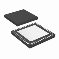
LMH0041SQ/NOPB National Semiconductor, LMH0041SQ/NOPB Datasheet - Page 12

LMH0041SQ/NOPB
Manufacturer Part Number
LMH0041SQ/NOPB
Description
IC DESERIALIZER SDI LVDS 48-LLP
Manufacturer
National Semiconductor
Series
LMH®r
Datasheet
1.LMH0051SQENOPB.pdf
(28 pages)
Specifications of LMH0041SQ/NOPB
Function
Deserializer
Data Rate
3Gbps
Input Type
Serial
Output Type
LVDS
Voltage - Supply
2.5V, 3.3V
Operating Temperature
-40°C ~ 85°C
Mounting Type
Surface Mount
Package / Case
48-LLP
Operating Temperature (min)
-40C
Operating Temperature Classification
Industrial
Operating Temperature (max)
85C
Package Type
LLP EP
Rad Hardened
No
Lead Free Status / RoHS Status
Lead free / RoHS Compliant
Number Of Outputs
-
Number Of Inputs
-
Lead Free Status / Rohs Status
Compliant
Other names
LMH0041SQTR
Available stocks
Company
Part Number
Manufacturer
Quantity
Price
www.national.com
SWITCHING SDI INPUTS
When the input to the DES is switched from one source to
another, either via the internal 2:1 multiplexor on the inputs,
or via an external crosspoint switch, there are a variety of be-
haviors possible If the input switch is between two signals
operating at the same datarate, then in most cases, the DES
will not lose lock. There will be a small number of words with
corrupted data as the PLL slews it's phase to match the new
input signal. Under some circumstances (dependent on
phase difference between the inputs, temperature, etc) it is
possible that the PLL will lose lock, and then reacquire lock.
This condition can be seen by monitoring the LOCK pin where
a high going pulse will indicate a loss of lock condition. If a
loss of lock happens, it will be for a time period of approxi-
mately 5ms before lock is reattained. In the invent that the
switch on the input is between signals at different datarates
— for example from a 270 Mbps signal to a 1.485 Gbps input,
then the lock procedure is much more complex, and the lock
time will be significantly longer. In either case, the IP that is
processing the received signal will need to reestablish the
proper framing of the words.
SDI OUTPUT INTERFACING
The serial loopthrough outputs provide low-skew comple-
mentary or differential signals. The output buffer is a current
mode design, and as such has a high impedance output. To
drive a 75Ω transmission line, a 75Ω resistor from each of the
output pins to V
two functions—it converts the current output to a voltage,
which is used to drive the cable, and it acts as the back ter-
mination resistor for the transmission line. The output driver
automatically adjusts its slew rate depending on the input
datarate so that it will be in compliance with SMPTE 259M,
SMPTE292M or SMPTE 424M as appropriate. In addition to
output amplitude and rise/fall time specifications, the SMPTE
specs require that SDI outputs meet an Output Return Loss
(ORL) specification. There are parasitic capacitances that will
be present both at the output pin of the device and on the
application printed circuit board. To optimize the return loss,
these must be compensated for, usually with a series network
comprising a parallel inductor and resistor. The actual values
for these components will vary from application to application,
FIGURE 4. Simplified SDI Input Circuit
DD2V5
should be connected. This resistor has
30017206
12
but the typical interface circuit shows values that would be a
good starting point.
JITTER MANAGEMENT
SMPTE 424M (the 3 Gbps standard) relaxed the require-
ments of SDI transmitters from 0.2UI to 0.3UI, which means
that the challenge of receiving these signals error free is very
difficult. The parameter of importance to determine if the DES
will be able to receive the signal error free is the Jitter Toler-
ance.
a 2.97 Gbps input — any signal which has less jitter than what
is on the upper curve of this figure will be able to be received
by the DES. The lower line in the curve shows the SMPTE
requirement for any receiver. There is a slight dip in the level
at frequencies abive about 10MHz which is an artifact of the
test equipment that was used to capture the data. Once the
signal is received, the next concern as far as jitter goes is how
much of the jitter that was on the input signal will be passed
through to the RXCLK output. This is answered by the Jitter
transfer characteristics. The Jitter transfer function is the ratio
of the input jitter to the output jitter, measured as a function of
frequency. The specification tables show two of the parame-
ters related to this curve — δ is the jitter peaking and indicates
what the maximum gain of the jitter is. Ideally δ is 0, but a
lower number is better. If several devices are used in a sys-
tem, and the frequency at which δ is maximum is the same
for all of them, then the gains will multiply, and there is a risk
that there will be excessive jitter accumulating at that fre-
quency. The LMH0341 has very low Jitter peaking, so this
should not be a concern. The other parameter of interest is
λ which is the jitter transfer bandwidth. Jitter on the input at
the frequency λ is attenuated by 3dB, and any jitter at fre-
quencies greater than λ is attenuated by more than this. From
a design standpoint, it means that you primarily only need to
worry about the jitter at frequencies below λ. The LMH0341
adjusts it's loop bandwidth dependent on datarate, so for the
lower datarates, it has a lower loop
the jitter transfer curve of an LMH0341 with a 2.97 Gbps signal
input, 0.5UI of input jitter, and nominal power supplies and
temperature.
Figure 8
FIGURE 5. Simplified SDI Output Circuit
shows the LMH0341 Jitter tolerance curve with
bandwidth.Figure 8
30017207
shows


