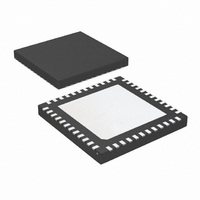
LMH0041SQ/NOPB National Semiconductor, LMH0041SQ/NOPB Datasheet - Page 13

LMH0041SQ/NOPB
Manufacturer Part Number
LMH0041SQ/NOPB
Description
IC DESERIALIZER SDI LVDS 48-LLP
Manufacturer
National Semiconductor
Series
LMH®r
Datasheet
1.LMH0051SQENOPB.pdf
(28 pages)
Specifications of LMH0041SQ/NOPB
Function
Deserializer
Data Rate
3Gbps
Input Type
Serial
Output Type
LVDS
Voltage - Supply
2.5V, 3.3V
Operating Temperature
-40°C ~ 85°C
Mounting Type
Surface Mount
Package / Case
48-LLP
Operating Temperature (min)
-40C
Operating Temperature Classification
Industrial
Operating Temperature (max)
85C
Package Type
LLP EP
Rad Hardened
No
Lead Free Status / RoHS Status
Lead free / RoHS Compliant
Number Of Outputs
-
Number Of Inputs
-
Lead Free Status / Rohs Status
Compliant
Other names
LMH0041SQTR
Available stocks
Company
Part Number
Manufacturer
Quantity
Price
SMBus INTERFACE
The configuration bus conforms to the System Management
Bus (SMBus) 2.0 specification. SMBus 2.0 includes multiple
options. The optional ARP (Address Resolution Protocol) fea-
ture is not supported. The I/O rail is 3.3V only and is not 5V
FIGURE 7. Jitter Transfer Curve Parameters
FIGURE 6. Jitter Tolerance Curve
FIGURE 8. Jitter Transfer Curve
30017221
30017220
30017213
13
tolerant. The use of the SMB_CS signal is recommended for
applications with multi-drop applications (multiple devices to
a host).
The System Management Bus (SMBus) is a two wire interface
designed for the communication between various system
component chips. By accessing the control functions of the
circuit via the SMBus, pin count is kept to a minimum while
allowing a maximum amount of versatility. The SMBus has
three pins to control it, there is an SMBus CS pin which en-
ables the SMBus interface for the device, a Clock and a Data
line. In applications where there might be several devices, the
SDA and SCK pins can be bussed together and the individual
devices to be communicated with may be selected via the CS
pin The SCL and SDA are both open drain and are pulled high
by external pullup resistors. The DES has several internal
configuration registers which may be accessed via the SM-
Bus. These registers are listed
Transfer Of Data To The Device Via The SMBus
During normal operation the data on SDA must be stable dur-
ing the time when SCK is high.
START / STOP / IDLE conditions—
There are three unique states for the SMBus:
START A HIGH to LOW transition on SDA while SCK is high
STOP
IDLE
SMBus Transactions
A transaction begins with the host placing the DES SMBus
into the START condition, then a byte (8 bits) is transferred,
MSB first, followed by a ninth ACK bit. ACK bits are ‘0’ to sig-
nify an ACK, or ‘1’ to signify NACK, after this the host holds
the SCL line low, and waits for the receiver to raise the SDA
line as an ACKnowledge that the byte has been received.
WRITING TO REGISTERS VIA THE SMBus INTERFACE
To write a data value to a register in the DES, the host writes
three bytes, the first byte is the device address—the device
address is a 7 bit value, and if writing to the DES the last bit
(LSB) is set to ‘0’ to signify that the operation is a write. The
second byte written is the register address, and the third byte
written is the data to be written into the addressed register. If
additional data writes are performed, the register address is
automatically incremented. At the end of the write cycle the
host places the bus in the STOP state.
READING FROM REGISTERS VIA THE SMBus
INTERFACE
To read the data value from a register, first the host writes the
device address with the LSB set to a ‘0’ denoting a write, then
the register address is written to the device. The host then
reasserts the START condition, and writes the device address
once again, but this time with the LSB set to a ‘1’ denoting a
read, and following this the DES will drive the SDA line with
the data from the addressed register. The host indicates that
it has finished reading the data by asserting a ‘1’ for the ACK
bit. After reading the last byte, the host will assert a ‘0’ for
NACK to indicate to the DES that it does not require any more
data.
indicates a message START condition,
A LOW to HIGH transition on SDA while SCK is high
indicates a message STOP condition.
If SCK and SDA are both high for a time exceeding
t
are high for a total exceeding the maximum specifi-
cation for t
state.
BUF
from the last detected STOP condition or if they
HIGH
then the bus will transfer to the IDLE
inDES Register Detail Table
www.national.com
.


