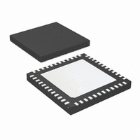
LMH0041SQ/NOPB National Semiconductor, LMH0041SQ/NOPB Datasheet - Page 21

LMH0041SQ/NOPB
Manufacturer Part Number
LMH0041SQ/NOPB
Description
IC DESERIALIZER SDI LVDS 48-LLP
Manufacturer
National Semiconductor
Series
LMH®r
Datasheet
1.LMH0051SQENOPB.pdf
(28 pages)
Specifications of LMH0041SQ/NOPB
Function
Deserializer
Data Rate
3Gbps
Input Type
Serial
Output Type
LVDS
Voltage - Supply
2.5V, 3.3V
Operating Temperature
-40°C ~ 85°C
Mounting Type
Surface Mount
Package / Case
48-LLP
Operating Temperature (min)
-40C
Operating Temperature Classification
Industrial
Operating Temperature (max)
85C
Package Type
LLP EP
Rad Hardened
No
Lead Free Status / RoHS Status
Lead free / RoHS Compliant
Number Of Outputs
-
Number Of Inputs
-
Lead Free Status / Rohs Status
Compliant
Other names
LMH0041SQTR
Available stocks
Company
Part Number
Manufacturer
Quantity
Price
ADD 'h Name
20
21
22
23–26
27
28
29–2A
Control
DVB_ASI
Override
Reserved
LVDS Control 1
LVDS Control 2
Reserved
Bits
7:3
2
1
0
This register allows the device to be placed in DVB_ASI mode or standard operation mode
7:5
4
3:2
1:0
This register allows the user to control the DVB_ASI and input select functions via the SMBus interface
rather than the pin controls.
7:5
4
3:1
0
This register allows control of the LVDS output pins — using this register individual LVDS outputs can
be enabled or disabled, and the outputs can be switched to high output mode
7
6
5
4
3
2
1
0
More bits allowing control over the LVDS outputs
7
6
5
4
3:2
1:0
Field
Reserved
Data Order
Reset Channel
Digital
Powerdown
Reserved
RX_MUX_SEL
Reserved
DVB_ASI
Reserved
RX_MUX
Control
Override
Reserved
DVB_ASI
Override
LVDS_VOD
LVDS Control
RXCLK Enable
RX4 Enable
RX3 Enable
RX2 Enable
RX1 Enable
RX0 Enable
Reserved
LVDS Reset
RXCLK Rate
RXCLK Invert
LVDS Clock
delay
Reserved
R/W
r/w
r/w
r/w
r/w
r/w
r/w
r/w
r/w
r/w
r/w
r/w
r/w
r/w
r/w
r/w
r/w
r/w
r/w
21
Default
10'b
0
0
0
0
0
0
0
0
0
0
0
0
0
0
0
1
0
Description
Determines deserialization order —
0: Expects LSB to be received first
1:Expects MSB to be received first
Writing a '1' to this bit forces a reset of the channel
Writing a '1' to this bit will shut down several of the
digital processing sections of the product to save
power.
If enabled by register 22, then this bit will override the
RX_MUX_SEL pin.
00,01,10: Standard Operation
11: DVB_ASI
Writing a '1' to this register allows register 21 to control
the state of the input multiplexer — if the bit is set to
'0' then the selection will be determined by the state
of the RX_MUX_SEL pin
Writing a '1' to this register allows register 21 to control
the state of the DVB_ASI Select pin — if the bit is set
to '0' then the selection will be determined by the state
of the DVB_ASI pin if '1' then the contents of register
21 take precidence
With a '0' the V
in the electrical characteristics table, writing a '1' to
this bit generates a larger V
to be driven, and increasing total power dissipation
Writing a '1' to this bit allows the LVDS outputs to be
controlled via the SMBus
Enables the RXCLK output driver
Enables RX4 output driver
Enables RX3 output driver
Enables RX2 output driver
Enables RX1 output driver
Enables RX0 output driver
Resets LVDS Block
1: RXCLK is a DDR clock
0: RXCLI is at a rate of DDR/2
Inverts the polarity of the RXCLK signal
Each LSB adds 80ps delay to the RXCLK signal path,
allowing the setup and hold times to be adjusted.
OD
of the LVDS output are as described
OD
allowing longer traces
www.national.com


