LM2506SQX/NOPB National Semiconductor, LM2506SQX/NOPB Datasheet - Page 6
LM2506SQX/NOPB
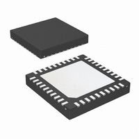
Manufacturer Part Number
LM2506SQX/NOPB
Description
IC SER/DESER 18BIT MPL 40-LLP
Manufacturer
National Semiconductor
Series
LMr
Datasheet
1.LM2506GRNOPB.pdf
(19 pages)
Specifications of LM2506SQX/NOPB
Function
Serializer/Deserializer
Data Rate
320Mbps
Input Type
LVCMOS
Output Type
LVCMOS
Number Of Inputs
22
Number Of Outputs
3
Voltage - Supply
1.74 V ~ 3 V
Operating Temperature
-30°C ~ 85°C
Mounting Type
Surface Mount
Package / Case
40-LLP
Lead Free Status / RoHS Status
Lead free / RoHS Compliant
Other names
LM2506SQX


www.national.com
SER PIXEL CLOCK (PCLK)
f
t
PCLK
t
t
CP
T
STOPpclk
Symbol
Recommended Input Timing Requirements
Over recommended operating supply and temperature ranges unless otherwise specified. (Note 2)
Note 1: “Absolute Maximum Ratings” are those values beyond which the safety of the device cannot be guaranteed. They are not meant to imply that the device
should be operated at these limits. The tables of “Electrical Characteristics” specify conditions for device operation.
Note 2: Typical values are given for V
Note 3: Current into a device pin is defined as positive. Current out of device pins is defined as negative. Voltages are referenced to Ground unless otherwise
specified.
Note 4: MPL Current Threshold is set to be 3XI
Note 5: Total Supply Current Conditions: RGB Mode, worse case data pattern, 13.3MHz PCLK, DES C
= 3.0V, MAX VDDA = VDDcore = 2.0V.
Note 6: Supply Current Conditions: RGB Mode, PRBS case data pattern, 13.3MHz PCLK, DES C
Note 7: Maximum transition time is a function of clock rate and should be less than 30% of the clock period to preserve signal quality.
Note 8: Guaranteed functionally by the I
Note 9: This is a functional parameter and is guaranteed by design or characterization.
Timing Diagrams
DC
Pixel Clock Frequency
Pixel Clock Period
Pixel Clock Duty Cycle
Transition Time
PClock Stop Gap
Parameter
DDIO
FIGURE 1. Serial Data Valid — DES Input Set and Hold Time
DDZ
= 1.8V and V
parameter. See also Figure 8.
FIGURE 2. DES Output Rise and Fall Time (PCLK)
B
by the MPL start up Sequence - this is a functional specification only.
(Note 7)
FIGURE 3. Stop Clock Power Down (SER)
DD
= V
DDA
= 1.8V and T
Conditions
6
A
= 25˚C.
L
= 15pF, TYP V
L
= 15pF, TYP V
75.2
Min
300
30
2
2
20125518
20125529
DDIO
DDIO
20125516
= V
= V
Typ
DDA
50
DDA
= V
= V
DDcore
DDcore
Max
13.3
500
= 1.8V.
70
= 1.8V, MAX VDDIO
Units
MHz
ns
ns
ns
%
Related parts for LM2506SQX/NOPB
Image
Part Number
Description
Manufacturer
Datasheet
Request
R

Part Number:
Description:
IC SER/DESER 18BIT MPL 4O-LLP
Manufacturer:
National Semiconductor
Datasheet:

Part Number:
Description:
National Semiconductor [8-Bit D/A Converter]
Manufacturer:
National Semiconductor
Datasheet:
Part Number:
Description:
National Semiconductor [Media Coprocessor]
Manufacturer:
National Semiconductor
Datasheet:
Part Number:
Description:
Digitally Controlled Tone and Volume Circuit with Stereo Audio Power Amplifier, Microphone Preamp Stage and National 3D Sound
Manufacturer:
National Semiconductor
Datasheet:
Part Number:
Description:
Digitally Controlled Tone and Volume Circuit with Stereo Audio Power Amplifier, Microphone Preamp Stage and National 3D Sound
Manufacturer:
National Semiconductor
Datasheet:
Part Number:
Description:
AC97 Rev 2 Codec with Sample Rate Conversion and National 3D Sound
Manufacturer:
National Semiconductor
Part Number:
Description:
Manufacturer:
National Semiconductor
Datasheet:
Part Number:
Description:
Manufacturer:
National Semiconductor
Datasheet:
Part Number:
Description:
General Purpose, Low Voltage, Low Power, Rail-to-Rail Output Operational Amplifiers
Manufacturer:
National Semiconductor
Datasheet:
Part Number:
Description:
8-bit 20 MSPS flash A/D converter.
Manufacturer:
National Semiconductor
Datasheet:
Part Number:
Description:
Low Noise Quad Operational Amplifier
Manufacturer:
National Semiconductor
Datasheet:
Part Number:
Description:
Quad Differential Line Receivers
Manufacturer:
National Semiconductor
Datasheet:
Part Number:
Description:
Quad High Speed Trapezoidal? Bus Transceiver
Manufacturer:
National Semiconductor
Datasheet:
Part Number:
Description:
Dual Line Receiver
Manufacturer:
National Semiconductor
Datasheet: