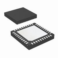
LM2506SQX/NOPB National Semiconductor, LM2506SQX/NOPB Datasheet - Page 8

LM2506SQX/NOPB
Manufacturer Part Number
LM2506SQX/NOPB
Description
IC SER/DESER 18BIT MPL 40-LLP
Manufacturer
National Semiconductor
Series
LMr
Datasheet
1.LM2506GRNOPB.pdf
(19 pages)
Specifications of LM2506SQX/NOPB
Function
Serializer/Deserializer
Data Rate
320Mbps
Input Type
LVCMOS
Output Type
LVCMOS
Number Of Inputs
22
Number Of Outputs
3
Voltage - Supply
1.74 V ~ 3 V
Operating Temperature
-30°C ~ 85°C
Mounting Type
Surface Mount
Package / Case
40-LLP
Lead Free Status / RoHS Status
Lead free / RoHS Compliant
Other names
LM2506SQX
www.national.com
Functional Description
The MPL start up sequence gives the DES an opportunity to
optimize the current sources in its receivers to maximize
noise margins. The SER begins the sequence by driving the
MC line logically Low for 180 MC cycles (t1). At this point, the
DES’s receiver samples the MC current flow and adjusts
itself to interpret that amount of current as a logical Low.
Once power is applied and stable, the PCLK should be
applied to the SER. Next the PD* inputs are driven High to
enable the SER and DES. The DES PD* input may be driven
High first, at the same time, or slightly later than the SER’s
PD* input. The SER’s PLL locks to the PCLK and the SER
drives the MC line to the 5I (Logic Low) state at point "A" for
t1. Next the SER drives the MC line to the 1I (Logic High)
state for t2. On the T1 to t2 transition - point "B", the DES
calibrates its current to that of the SER to maximize noise
margins. Next the SER drives the MC and MD lines to the 5I
(logic Low) state for t3. At point "C", video data is now
sampled and streamed to the DES.
OFF PHASE
In the OFF phase, both SER and DES MPL transmitters are
turned off with zero current flowing on the MC and MDn
lines. Figure 8 shows the transition of the MPL bus into the
OFF phase. If an MPL line is driven to a logical Low (high
current) when the OFF phase is entered it may temporarily
pass through as a logical High (low current) before reaching
the zero line current state.
(Continued)
FIGURE 7. Bus Power Up Timing
8
Next the SER drives the MC line logically HIGH for 180 MC
cycles (t2). The optimized current configuration is held as
long as the MPL remains active. Next, the SER drives both
the MC and the MD lines to a logical Low for another 180 MC
cycles (t3), after which it begins to toggle the MC line at 6X
the PCLK rate. The SER will continue to toggle the MC line
as long as its PD* pin remains de-asserted (High). At this
point, video data is streaming to the DES.
RGB VIDEO INTERFACE
The LM2506 is transparent to data format and control signal
timing. Each PCLK, data inputs, HS, VS and DE are
sampled. A PCLK by PCLK representation of these signals is
duplicated on the opposite device after being transferred
across the MPL Level-0 interface.
The LM2506 uses a multiple range PLL and an on-chip
multiplier to accommodate a wide range of display formats.
QVGA to
MHz PCLK input range.
Pixel Bandwidth = H. X V. X Color Depth X Frames
1
⁄
FIGURE 8. Bus Power Down Timing
2
SVGA can be supported within the 2 MHz to 13.3
20125561
20125506


