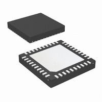
LM2506SQX/NOPB National Semiconductor, LM2506SQX/NOPB Datasheet - Page 7

LM2506SQX/NOPB
Manufacturer Part Number
LM2506SQX/NOPB
Description
IC SER/DESER 18BIT MPL 40-LLP
Manufacturer
National Semiconductor
Series
LMr
Datasheet
1.LM2506GRNOPB.pdf
(19 pages)
Specifications of LM2506SQX/NOPB
Function
Serializer/Deserializer
Data Rate
320Mbps
Input Type
LVCMOS
Output Type
LVCMOS
Number Of Inputs
22
Number Of Outputs
3
Voltage - Supply
1.74 V ~ 3 V
Operating Temperature
-30°C ~ 85°C
Mounting Type
Surface Mount
Package / Case
40-LLP
Lead Free Status / RoHS Status
Lead free / RoHS Compliant
Other names
LM2506SQX
OFF (O)
ACTIVE (A)
LINK-UP (LU)
Timing Diagrams
Functional Description
BUS OVERVIEW
The LM2506 is a dual link SER/DES configurable part that
supports an 18-bit RGB Display interface. The MPL physical
layer is purpose-built for an extremely low power and low
EMI data transmission while requiring the fewest number of
signal lines. No external line components are required, as
termination is provided internal to the MPL receiver. A maxi-
mum raw throughput of 320 Mbps (raw) is possible with this
chipset. When the protocol overhead is taken into account, a
maximum data throughput of 240 Mbps is possible. The MPL
interface is designed for use with common 50Ω to 100Ω lines
using standard materials and connectors. Lines may be
microstrip or stripline construction. Total length of the inter-
connect is expected to be less than 20cm.
Notes on MC/MD Line State:
0 = no current (off)
L = Logic Low — The higher level of current on the MC and MD lines
H = Logic High — The lower level of current on the MC and MD lines
X = Low or High
A = Active Clock
SERIAL BUS START UP TIMING
In the Serial Bus OFF phase, SER transmitters for MD0,
MD1 and MC are turned off such that zero current flows over
the MPL lines. In addition, both the SER and the DES are
internally held in a low power state. When the PD* input pins
Name
FIGURE 5. MPL Point-to-Point Bus
MC State
(Continued)
A
H
0
FIGURE 4. Stop Clock Power Up (SER)
20125502
MDn State
X
0
-
TABLE 1. Link Phases
Link is Off
Data Out
SER initiated Link-Up
7
SERIAL BUS TIMING
Data valid is relative to both edges for a RGB transaction as
shown in Figure 6. Data valid is specified as: Data Valid
before Clock, Data Valid after Clock, and Skew between
data lines should be less than 500ps.
SERIAL BUS PHASES
There are three bus phases on the MPL serial bus. These
are determined by the state of the MC and MD lines. The
MPL bus phases are shown in Table 1.
The LM2506 supports MPL Level 0 Enhanced Protocol with
a Class 0 PHY.
Phase Description
are de-asserted (driven High) the SER enables its PLL and
waits for enough time to pass for its PLL to lock. After the
SER’s PLL is locked (t0 = 4,096 PCLK Cycles), the SER will
perform an MPL start up sequence. The DES will power up
and await the start up sequence from the SER once its PD*
input is driven High.
FIGURE 6. Dual Link Timing (WRITE)
20125530
Pre-Phase
LU, A, or I
A, I or LU
O
20125503
Post-Phase
www.national.com
A, I, or O
A, I, or O
LU


