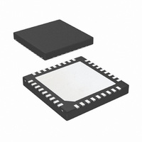
DS25MB100TSQ/NOPB National Semiconductor, DS25MB100TSQ/NOPB Datasheet - Page 4

DS25MB100TSQ/NOPB
Manufacturer Part Number
DS25MB100TSQ/NOPB
Description
IC MUX/BUFFER 1:2 2.5GBPS 36-LLP
Manufacturer
National Semiconductor
Type
MUXr
Datasheet
1.DS25MB100TSQNOPB.pdf
(14 pages)
Specifications of DS25MB100TSQ/NOPB
Tx/rx Type
CML
Delay Time
1.0ns
Voltage - Supply
3.135 V ~ 3.465 V
Mounting Type
Surface Mount
Package / Case
36-LLP
For Use With
DS25MB100EVK - KIT EVAL FOR DS25MB100
Lead Free Status / RoHS Status
Lead free / RoHS Compliant
Current - Supply
-
Capacitance - Input
-
Other names
DS25MB100TSQTR
Available stocks
Company
Part Number
Manufacturer
Quantity
Price
Company:
Part Number:
DS25MB100TSQ/NOPB
Manufacturer:
NSC
Quantity:
895
www.national.com
Connection Diagram
Functional Description
The DS25MB100 is a signal conditioning 2:1 multiplexer and
a 1:2 buffer designed to support port redundancy up to 2.5
Gbps. The high speed inputs are self-biased to about 1.3V
and are designed for AC coupling. The inputs are compatible
to most AC coupling differential signals such as LVDS,
LVPECL and CML. The DS25MB100 is not designed to op-
erate with data rates below 250 Mbps or with a DC bias
applied to the CML inputs or outputs. Most high speed links
are encoded for DC balance and have been defined to include
AC coupling capacitors allowing the DS25MB100 to be di-
rectly inserted into the datapath without any limitation. The
ideal AC coupling capacitor value is often based on the lowest
frequency component embedded within the serial link. A typ-
ical AC coupling capacitor value ranges between 100 and
1000nF, some specifications with scrambled data may re-
quire a larger capacitor for optimal performance. To reduce
unwanted parasitics around and within the AC coupling ca-
pacitor, a body size of 0402 is recommended. Figure 5 shows
the AC coupling capacitor placement in an AC test circuit.
Each input stage has a fixed equalizer that provides equal-
ization to compensate about 5 dB of transmission loss from a
short backplane trace (about 10 inches backplane). The out-
put driver has Pre-emphasis (driver-side equalization) to
compensate the transmission loss of the backplane that it is
driving. The driver conditions the output signal such that the
lower frequency and higher frequency pulses reach approxi-
See NS Package Number SQA36A
Order Number DS25MB100TSQ
4
mately the same amplitude at the end of the backplane, and
minimize the deterministic jitter caused by the amplitude dis-
parity. The DS25MB100 provides four steps of user-se-
lectable Pre-emphasis ranging from 0, -3, -6 and –9 dB to
handle different lengths of backplane. Figure 1 shows a driver
Pre-emphasis waveform. The Pre-emphasis duration is
188ps nominal, corresponds to 0.47 bit-width at 2.5 Gbps.
The Pre-emphasis levels of switch-side and line-side can be
individually programmed.
MUX
0
1
(default)
LB0
0
1
(default)
LB1
0
1
(default)
TABLE 2. Logic Table For Loopback Controls
TABLE 1. Logic Table For Multiplex Controls
Loopback Function
Enable loopback from IN0± to OUT0±.
Normal mode. Loopback disabled.
Loopback Function
Enable loopback from IN1± to OUT1±.
Normal mode. Loopback disabled.
Mux Function
MUX select switch input, IN1±.
MUX select switch input, IN0±.
20208903


