DS25MB100TSQ/NOPB National Semiconductor, DS25MB100TSQ/NOPB Datasheet - Page 7
DS25MB100TSQ/NOPB
Manufacturer Part Number
DS25MB100TSQ/NOPB
Description
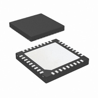
IC MUX/BUFFER 1:2 2.5GBPS 36-LLP
Manufacturer
National Semiconductor
Type
MUXr
Datasheet
1.DS25MB100TSQNOPB.pdf
(14 pages)
Specifications of DS25MB100TSQ/NOPB
Tx/rx Type
CML
Delay Time
1.0ns
Voltage - Supply
3.135 V ~ 3.465 V
Mounting Type
Surface Mount
Package / Case
36-LLP
For Use With
DS25MB100EVK - KIT EVAL FOR DS25MB100
Lead Free Status / RoHS Status
Lead free / RoHS Compliant
Current - Supply
-
Capacitance - Input
-
Other names
DS25MB100TSQTR
Available stocks
Company
Part Number
Manufacturer
Quantity
Price
Company:

Part Number:
DS25MB100TSQ/NOPB
Manufacturer:
NSC
Quantity:
895


T
R
R
ΔR
V
POWER DISSIPATION
P
AC CHARACTERISTICS
t
t
t
t
t
t
t
t
RJ
DJ
DR
Symbol
R
F
PLH
PHL
SKP
SKO
SKPP
SM
PE
OCM
D
OTSE
OTD
Note 1: “Absolute Maximum Ratings” are the ratings beyond which the safety of the device cannot be guaranteed. They are not meant to imply that the device
should be operated at these limits.
Note 2: Typical parameters measured at V
specifications are not guaranteed.
Note 3: IN+ and IN− are generic names refer to one of the many pairs of complimentary inputs of the DS25MB100. OUT+ and OUT− are generic names refer to
one of the many pairs of the complimentary outputs of the DS25MB100. Differential input voltage V
defined as |OUT+–OUT−|.
OTSE
Pre-Emphasis Width
Output Termination (Note
3)
Output Differential
Termination
Mis-Match in Output
Termination Resistors
Output Common Mode
Voltage
Power Dissipation
Differential Low to High
Transition Time
Differential High to Low
Transition Time
Differential Low to High
Propagation Delay
Differential High to Low
Propagation Delay
Pulse Skew
Output Skew
(Note 7)
Part-to-Part Skew
Mux Switch Time
Device Random Jitter
(Note 5)
Device Deterministic Jitter
(Note 6)
Data Rate (Note 9)
Parameter
CC
Tested at −9 dB Pre-emphasis level, DEx[1:0]=11
x=S for switch side Pre-emphasis control
x=L for line side Pre-emphasis control
See Figure 4 on measurement condition.
On-chip termination from OUT+ or OUT− to V
On-chip differential termination between OUT+ and
OUT−
Mis-match in output terminations at OUT+ and OUT−
V
All outputs terminated by 100Ω ±1%.
DEL_[1:0]=0, DES_[1:0]=0
Running PRBS 2
Measured with a clock-like pattern at 2.5 Gbps,
between 20% and 80% of the differential output
voltage. Pre-emphasis disabled
Transition time is measured with fixture as shown in
Figure 5, adjusted to reflect the transition time at the
output pins
Measured at 50% differential voltage from input to
output
|t
Difference in propagation delay between two outputs
in the same device
Difference in propagation delay between the same
output from devices operating under identical
conditions
Measured from V
loopback control to 50% of the valid differential output
See Figure 5 for test circuit.
Alternating-1-0 pattern
EQ and Pre-emphasis disabled.
At 0.25 Gbps
At 1.25 Gbps
At 2.5 Gbps
See Figure 5 for test circuit.
EQ and Pre-emphasis disabled
Between 0.25 and 2.5 Gbps with PRBS7 pattern for
DS25MB100 @ –40°C to 85°C
Tested with alternating-1-0 pattern
PHL
DD
= 3.3V, T
–t
= 3.3V @ 25°C
PLH
A
|
= 25°C, and represent most likely parametric norms at the time of product characterization. The typical
7
IH
-1 pattern at 2.5 Gbps
or V
Conditions
IL
of the mux-control or
7
ID
CC
is defined as |IN+–IN−|. Differential output voltage V
0.25
Min
125
42
(Note 2)
0.45
Typ
188
100
100
100
2.7
1.8
50
Max
250
100
100
2.5
58
20
35
5
1
1
6
2
2
2
www.national.com
psrms
psrms
psrms
Units
Gbps
Pspp
ps
ps
ps
ns
ns
ps
ps
ps
ns
OD
%
W
Ω
Ω
V
is
Related parts for DS25MB100TSQ/NOPB
Image
Part Number
Description
Manufacturer
Datasheet
Request
R

Part Number:
Description:
National Semiconductor [8-Bit D/A Converter]
Manufacturer:
National Semiconductor
Datasheet:
Part Number:
Description:
National Semiconductor [Media Coprocessor]
Manufacturer:
National Semiconductor
Datasheet:
Part Number:
Description:
Digitally Controlled Tone and Volume Circuit with Stereo Audio Power Amplifier, Microphone Preamp Stage and National 3D Sound
Manufacturer:
National Semiconductor
Datasheet:
Part Number:
Description:
Digitally Controlled Tone and Volume Circuit with Stereo Audio Power Amplifier, Microphone Preamp Stage and National 3D Sound
Manufacturer:
National Semiconductor
Datasheet:
Part Number:
Description:
AC97 Rev 2 Codec with Sample Rate Conversion and National 3D Sound
Manufacturer:
National Semiconductor
Part Number:
Description:
Manufacturer:
National Semiconductor
Datasheet:
Part Number:
Description:
Manufacturer:
National Semiconductor
Datasheet:
Part Number:
Description:
General Purpose, Low Voltage, Low Power, Rail-to-Rail Output Operational Amplifiers
Manufacturer:
National Semiconductor
Datasheet:
Part Number:
Description:
8-bit 20 MSPS flash A/D converter.
Manufacturer:
National Semiconductor
Datasheet:
Part Number:
Description:
Low Noise Quad Operational Amplifier
Manufacturer:
National Semiconductor
Datasheet:
Part Number:
Description:
Quad Differential Line Receivers
Manufacturer:
National Semiconductor
Datasheet:
Part Number:
Description:
Quad High Speed Trapezoidal? Bus Transceiver
Manufacturer:
National Semiconductor
Datasheet:
Part Number:
Description:
Dual Line Receiver
Manufacturer:
National Semiconductor
Datasheet:
Part Number:
Description:
TTL to 10k ECL Level Translator with Latch
Manufacturer:
National Semiconductor
Datasheet: