DS25MB100TSQ/NOPB National Semiconductor, DS25MB100TSQ/NOPB Datasheet - Page 8
DS25MB100TSQ/NOPB
Manufacturer Part Number
DS25MB100TSQ/NOPB
Description
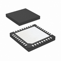
IC MUX/BUFFER 1:2 2.5GBPS 36-LLP
Manufacturer
National Semiconductor
Type
MUXr
Datasheet
1.DS25MB100TSQNOPB.pdf
(14 pages)
Specifications of DS25MB100TSQ/NOPB
Tx/rx Type
CML
Delay Time
1.0ns
Voltage - Supply
3.135 V ~ 3.465 V
Mounting Type
Surface Mount
Package / Case
36-LLP
For Use With
DS25MB100EVK - KIT EVAL FOR DS25MB100
Lead Free Status / RoHS Status
Lead free / RoHS Compliant
Current - Supply
-
Capacitance - Input
-
Other names
DS25MB100TSQTR
Available stocks
Company
Part Number
Manufacturer
Quantity
Price
Company:

Part Number:
DS25MB100TSQ/NOPB
Manufacturer:
NSC
Quantity:
895


www.national.com
Note 4: K28.7 pattern is a 10-bit repeating pattern of K28.7 code group {001111 1000}
K28.5 pattern is a 20-bit repeating pattern of +K28.5 and −K28.5 code groups {110000 0101 001111 1010}
Note 5: Device output random jitter is a measurement of the random jitter contribution from the device. It is derived by the equation sqrt(RJ
RJ
Note 6: Device output deterministic jitter is a measurement of the deterministic jitter contribution from the device. It is derived by the equation (DJ
DJ
driving the device.
Note 7: t
IN1± to OUT±. Another example is the output skew among data paths from IN± to OUT0± and IN± to OUT1±. t
paths of the same port and between similar data paths. An example is the output skew among data paths IN0± to OUT0± and IN1± to OUT1±.
Note 8: Thermal resistances are based on having 16 thermal relief vias on the DAP pad under the 0 airflow condition.
Note 9: This parameter is guaranteed by design and/or characterization. It is not tested in production.
Note 10: ESD tests conform to the following standards:
Timing Diagrams
OUT
OUT
is the total peak-to-peak deterministic jitter measured at the output of the device in pspp, DJ
is the total random jitter measured at the output of the device in psrms, RJ
SKO
Human Body Model applicable standard: MIL-STD-883, Method 3015.7
Machine Model applicable standard: JESD22-A115-A (ESD MM standard of JEDEC)
Field-induced Charge Device Model: Applicable standard JESD22-C101-C (ESD FICDM standard of JEDEC)
is the magnitude difference in the propagation delays among data paths. An example is the output skew among data paths from IN0± to OUT± and
FIGURE 3. Propagation Delay from Input to Output
FIGURE 2. Driver Output Transition Time
8
IN
is the random jitter of the pattern generator driving the device.
IN
is the peak-to-peak deterministic jitter of the pattern generator
20208905
SKO
also refers to the delay skew of the loopback
20208906
OUT
OUT
2
– RJ
–DJ
IN
2
IN
), where
), where
Related parts for DS25MB100TSQ/NOPB
Image
Part Number
Description
Manufacturer
Datasheet
Request
R

Part Number:
Description:
National Semiconductor [8-Bit D/A Converter]
Manufacturer:
National Semiconductor
Datasheet:
Part Number:
Description:
National Semiconductor [Media Coprocessor]
Manufacturer:
National Semiconductor
Datasheet:
Part Number:
Description:
Digitally Controlled Tone and Volume Circuit with Stereo Audio Power Amplifier, Microphone Preamp Stage and National 3D Sound
Manufacturer:
National Semiconductor
Datasheet:
Part Number:
Description:
Digitally Controlled Tone and Volume Circuit with Stereo Audio Power Amplifier, Microphone Preamp Stage and National 3D Sound
Manufacturer:
National Semiconductor
Datasheet:
Part Number:
Description:
AC97 Rev 2 Codec with Sample Rate Conversion and National 3D Sound
Manufacturer:
National Semiconductor
Part Number:
Description:
Manufacturer:
National Semiconductor
Datasheet:
Part Number:
Description:
Manufacturer:
National Semiconductor
Datasheet:
Part Number:
Description:
General Purpose, Low Voltage, Low Power, Rail-to-Rail Output Operational Amplifiers
Manufacturer:
National Semiconductor
Datasheet:
Part Number:
Description:
8-bit 20 MSPS flash A/D converter.
Manufacturer:
National Semiconductor
Datasheet:
Part Number:
Description:
Low Noise Quad Operational Amplifier
Manufacturer:
National Semiconductor
Datasheet:
Part Number:
Description:
Quad Differential Line Receivers
Manufacturer:
National Semiconductor
Datasheet:
Part Number:
Description:
Quad High Speed Trapezoidal? Bus Transceiver
Manufacturer:
National Semiconductor
Datasheet:
Part Number:
Description:
Dual Line Receiver
Manufacturer:
National Semiconductor
Datasheet:
Part Number:
Description:
TTL to 10k ECL Level Translator with Latch
Manufacturer:
National Semiconductor
Datasheet: