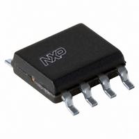
PCA9509D,112 NXP Semiconductors, PCA9509D,112 Datasheet - Page 8

PCA9509D,112
Manufacturer Part Number
PCA9509D,112
Description
IC I2C BUS REPEATER 8-SOIC
Manufacturer
NXP Semiconductors
Type
Repeaterr
Datasheet
1.PCA9509DP118.pdf
(19 pages)
Specifications of PCA9509D,112
Tx/rx Type
I²C Logic
Delay Time
109ns
Capacitance - Input
2pF
Voltage - Supply
3 V ~ 5.5 V
Current - Supply
5mA
Mounting Type
Surface Mount
Package / Case
8-SOIC (3.9mm Width)
Lead Free Status / RoHS Status
Lead free / RoHS Compliant
Other names
568-3355-5
935282227112
PCA9509D
935282227112
PCA9509D
NXP Semiconductors
[2]
[3]
[4]
[5]
[6]
PCA9509_5
Product data sheet
Fig 8.
If the PCA9509 is not being enabled or disabled, the V
below the minimum specification of 450 A at cold temperature (see
and fall times of the signals on port A since the I
capacitance will result in a slower rise time and a longer transition time in general, however since the lower current is also associated
with a lower voltage swing the delay is somewhat compensated. The key point of the graphs is that the current has a temperature
dependence, and the output driver will also have the same temperature dependency so that the output offset of ~200 mV on port A is
nearly temperature independent. Even though the I
400 A instead of 450 A at cold temperature, the output is designed to be somewhat resistive such that under nominal conditions
(1.1 V) the current source pull-up will source 1 mA and the output pull-down will sink the 1 mA at ~200 mV, so as the current source
current decreases the output pull-down resistance increases in order to maintain the offset.
V
port B output staying LOW.
The port A current source has a typical value of about 1 mA, but varies with both V
port A current source current drops to 0 mA. The current source current dropping across the internal pull-down driver resistance of
about 200
As long as the chip ground is common with the input ground reference the driver resistance may be as large as 120 . However, ground
offset will rapidly decrease the maximum allowed driver resistance.
Guaranteed by design.
(mA)
IL
I
(1) High limit
(2) Maximum
(3) Mean
(4) Minimum
(5) Low limit
IL
0.4
0.8
1.2
1.6
specification is for the falling edge seen by the port A input. V
0
40
Pins under test = An pins
LOW-level input current as a function of
temperature; V
(1)
(5)
defines the V
(3)
CC(A)
OL
(2)
(4)
.
25
= 1.0 V
T
amb
002aae733
( C)
IL
value represents the current source pull-up current, so a lower current into the same
IL
85
Rev. 05 — 10 July 2009
parameter indicates that at V
CC(A)
minimum is 0.95 V with a corresponding decrease in the I
ILc
Fig 9.
is for the static LOW levels seen by the port A input resulting in
Figure 8
(mA)
I
(1) High limit
(2) Maximum
(3) Mean
(4) Minimum
(5) Low limit
IL
0.4
0.8
1.2
1.6
0
40
Pins under test = An pins
LOW-level input current as a function of
temperature; V
and
Level translating I
CC(A)
CC(A)
Figure
of 0.95 V the PCA9509 can only sink up to
and V
9). This will not significantly change the rise
CC(B)
CC(A)
. Below V
25
= 0.95 V
2
C-bus/SMBus repeater
(2)
(3)
(4)
CC(A)
PCA9509
© NXP B.V. 2009. All rights reserved.
T
of about 0.7 V the
amb
002aae734
IL
( C)
, which will drop
(1)
(5)
85
8 of 19


