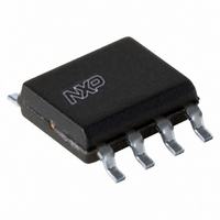
PCA9517AD,118 NXP Semiconductors, PCA9517AD,118 Datasheet - Page 3

PCA9517AD,118
Manufacturer Part Number
PCA9517AD,118
Description
IC I2C BUS REPEATER 8-SOIC
Manufacturer
NXP Semiconductors
Type
Repeaterr
Specifications of PCA9517AD,118
Package / Case
8-SOIC (3.9mm Width)
Mounting Type
Surface Mount
Current - Supply
5mA
Voltage - Supply
2.7 V ~ 5.5 V
Delay Time
170ns
Capacitance - Input
6pF
Tx/rx Type
I²C Logic
Supply Voltage (max)
5.5 V
Supply Voltage (min)
0.9 V
Maximum Operating Temperature
+ 85 C
Minimum Operating Temperature
- 40 C
Mounting Style
SMD/SMT
Number Of Circuits
Dual
Lead Free Status / RoHS Status
Lead free / RoHS Compliant
Lead Free Status / RoHS Status
Lead free / RoHS Compliant, Lead free / RoHS Compliant
Other names
935285763118::PCA9517AD-T::PCA9517AD-T
NXP Semiconductors
5. Pinning information
6. Functional description
PCA9517_3
Product data sheet
5.1 Pinning
5.2 Pin description
Table 2.
Refer to
The PCA9517 enables I
without degradation of system performance. The PCA9517 contains two bidirectional
open-drain buffers specifically designed to support up-translation/down-translation
between the low voltage (as low as 0.9 V) and a 3.3 V or 5 V I
and I/Os are overvoltage tolerant to 5.5 V even when the device is unpowered (V
and/or V
drivers turned off until V
can be applied in any sequence at power-up. After power-up and with the enable (EN)
HIGH, a LOW level on the A-side (below 0.3V
(either SDA or SCL) on and drives the B-side down to about 0.5 V. When the A-side rises
above 0.3V
pulls the pin HIGH. When the B-side falls first and goes below 0.3V
turned on and the A-side pulls down to 0 V. The B-side pull-down is not enabled unless
the B-side voltage goes below 0.4 V. If the B-side low voltage does not go below 0.5 V, the
A-side driver will turn off when the B-side voltage is above 0.7V
voltage goes below 0.4 V, the B-side pull-down driver is enabled and the B-side will only
Symbol
V
SCLA
SDAA
GND
EN
SDAB
SCLB
V
Fig 2. Pin configuration for SO8
CCA
CCB
SDAA
SCLA
V
CCA
Figure 1 “Functional diagram of
GND
CCA
Pin description
CCA
= 0 V). The PCA9517 includes a power-up circuit that keeps the output
1
2
3
4
Pin
1
2
3
4
5
6
7
8
the B-side pull-down driver is turned off and the external pull-up resistor
PCA9517D
002aac198
Rev. 03 — 30 January 2007
2
CCB
C-bus or SMBus translation down to V
is above 2.5 V and the V
Description
A-side supply voltage (0.9 V to 5.5 V)
serial clock A-side bus
serial data A-side bus
supply ground (0 V)
active HIGH repeater enable input
serial data B-side bus
serial clock B-side bus
B-side supply voltage (2.7 V to 5.5 V)
8
7
6
5
V
SCLB
SDAB
EN
CCB
PCA9517”.
CCA
Fig 3. Pin configuration for TSSOP8
) turns the corresponding B-side driver
SDAA
SCLA
V
GND
CCA
(MSOP8)
Level translating I
CCA
is above 0.8 V. V
1
2
3
4
2
PCA9517DP
C-bus or SMBus. All inputs
CCB
CCA
CCB
. If the B-side low
as low as 0.9 V
002aac199
PCA9517
the A-side driver is
© NXP B.V. 2007. All rights reserved.
2
C-bus repeater
CCB
8
7
6
5
V
SCLB
SDAB
EN
and V
CCB
CCB
3 of 19
CCA


