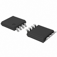
PCA9517ADP,118 NXP Semiconductors, PCA9517ADP,118 Datasheet - Page 5

PCA9517ADP,118
Manufacturer Part Number
PCA9517ADP,118
Description
IC I2C BUS REPEATER 8-TSSOP
Manufacturer
NXP Semiconductors
Type
Repeaterr
Datasheet
1.PCA9517AD118.pdf
(19 pages)
Specifications of PCA9517ADP,118
Package / Case
8-TSSOP
Mounting Type
Surface Mount
Current - Supply
5mA
Voltage - Supply
2.7 V ~ 5.5 V
Delay Time
170ns
Capacitance - Input
6pF
Tx/rx Type
I²C Logic
Supply Voltage (max)
5.5 V
Supply Voltage (min)
0.9 V
Maximum Operating Temperature
+ 85 C
Minimum Operating Temperature
- 40 C
Mounting Style
SMD/SMT
Number Of Circuits
Dual
Lead Free Status / RoHS Status
Lead free / RoHS Compliant
Lead Free Status / RoHS Status
Lead free / RoHS Compliant, Lead free / RoHS Compliant
Other names
935285764118::PCA9517ADP-T::PCA9517ADP-T
NXP Semiconductors
7. Application design-in information
PCA9517_3
Product data sheet
A typical application is shown in
on a 3.3 V I
Master devices can be placed on either bus.
The PCA9517 is 5 V tolerant, so it does not require any additional circuitry to translate
between 0.9 V to 5.5 V bus voltages and 2.7 V to 5.5 V bus voltages.
When the A-side of the PCA9517 is pulled LOW by a driver on the I
detects the falling edge when it goes below 0.3V
B-side to turn on, causing the B-side to pull down to about 0.5 V. When the B-side of the
PCA9517 falls, first a CMOS hysteresis type input detects the falling edge and causes the
internal driver on the A-side to turn on and pull the A-side pin down to ground. In order to
illustrate what would be seen in a typical application, refer to
bus master in
in
except that the HIGH level may be as low as 0.9 V, and the turn on and turn off of the
acknowledge signals are slightly delayed.
On the B bus side of the PCA9517, the clock and data lines would have a positive offset
from ground equal to the V
be pulled to the V
the end of the acknowledge, the level rises only to the LOW level set by the driver in the
PCA9517 for a short delay while the A bus side rises above 0.3V
HIGH. It is important to note that any arbitration or clock stretching events require that the
LOW level on the B bus side at the input of the PCA9517 (V
recognized by the PCA9517 and then transmitted to the A bus side.
Multiple PCA9517 A-sides can be connected in a star configuration
nodes to communicate with each other.
Multiple PCA9517s can be connected in series
connected to the B-side. I
segments. The number of devices that can be connected in series is limited by repeater
delay/time-of-flight considerations on the maximum bus speed requirements.
Fig 4. Typical application
Figure 8
would be observed on the A bus. This looks like a normal I
2
C-bus while the slave is connected to a 1.2 V bus. Both buses run at 400 kHz.
Figure 4
OL
MASTER
400 kHz
BUS
of the slave device which is very close to ground in this example. At
Rev. 03 — 30 January 2007
SDA
SCL
were to write to the slave through the PCA9517, waveforms shown
10 k
2
C-bus slave devices can be connected to any of the bus
OL
bus B
3.3 V
of the PCA9517. After the 8th clock pulse, the data line will
Figure
10 k
SDAB
SCLB
EN
V
4. In this example, the system master is running
CCB
PCA9517
V
(Figure
CCA
CCA
SDAA
SCLA
10 k
and causes the internal driver on the
Level translating I
6) as long as the A-side is
bus A
1.2 V
IL
10 k
Figure 8
) be at or below 0.4 V to be
SDA
SCL
CCA
400 kHz
SLAVE
002aac201
(Figure
2
C-bus, a comparator
2
then it continues
C-bus transmission
and
PCA9517
© NXP B.V. 2007. All rights reserved.
2
C-bus repeater
Figure
5), allowing all
9. If the
5 of 19


