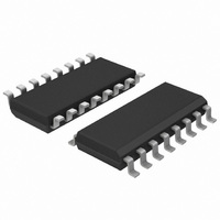
PCA9516D,118 NXP Semiconductors, PCA9516D,118 Datasheet - Page 6

PCA9516D,118
Manufacturer Part Number
PCA9516D,118
Description
IC I2C BUS HUB 5-CH 16SOIC
Manufacturer
NXP Semiconductors
Type
Bufferr
Datasheet
1.PCA9516PW112.pdf
(12 pages)
Specifications of PCA9516D,118
Tx/rx Type
I²C Logic
Delay Time
75ns
Capacitance - Input
6pF
Voltage - Supply
2.3 V ~ 3.6 V
Current - Supply
5mA
Mounting Type
Surface Mount
Package / Case
16-SOIC (3.9mm Width)
Lead Free Status / RoHS Status
Lead free / RoHS Compliant
Other names
935268880118
PCA9516D-T
PCA9516D-T
PCA9516D-T
PCA9516D-T
Philips Semiconductors
In order to illustrate what would be seen in a typical application,
refer to Figures 5 and 6. If the bus master in Figure 4 were to write
to the slave through the PCA9516, we would see the waveform
shown in Figure 5 on Bus 0. This looks like a normal I
transmission until the falling edge of the 8th clock pulse. At that
point, the master releases the data line (SDA) while the slave pulls it
LOW through the PCA9516. Because the V
typically around 0.5 V, a step in the SDA will be seen. After the
master has transmitted the 9th clock pulse, the slave releases the
data line.
2006 Sep 22
5-channel I
V
OL
OF MASTER
2
C hub
9th CLOCK PULSE
9th CLOCK PULSE
OL
of the PCA9516 is
V
2
C
OL
OF SLAVE
Figure 5. Bus 0 waveform
Figure 6. Bus 1 waveform
6
On the Bus 1 side of the PCA9516, the clock and data lines would
have a positive offset from ground equal to the V
After the 8th clock pulse, the data line will be pulled to the V
slave device that is very close to ground in our example.
It is important to note that any arbitration or clock stretching events
on Bus 1 require that the V
below the V
Characteristics section) to be recognized by the PCA9516 and then
transmitted to Bus 0.
OL
of the PCA9516 (see V
V
OL
OL
OF PCA9516
of the devices on Bus 1 be 70 mV
V
OL
OF PCA9516
OL
– V
2 V/DIV
2 V/DIV
ilc
in the DC
OL
PCA9516
Product data sheet
of the PCA9516.
SW00966
SW00965
OL
of the


