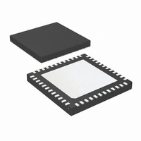
LMH0070SQE/NOPB National Semiconductor, LMH0070SQE/NOPB Datasheet - Page 12

LMH0070SQE/NOPB
Manufacturer Part Number
LMH0070SQE/NOPB
Description
IC SERIALIZER/CABLE DVR 48-LLP
Manufacturer
National Semiconductor
Datasheet
1.LMH0070SQENOPB.pdf
(26 pages)
Specifications of LMH0070SQE/NOPB
Applications
Displays
Interface
SMBus (2-Wire/I²C)
Voltage - Supply
3.135 V ~ 3.465 V
Package / Case
48-LLP
Mounting Type
Surface Mount
Lead Free Status / RoHS Status
Lead free / RoHS Compliant
Other names
LMH0070SQE
LMH0070SQE
LMH0070SQETR
LMH0070SQE
LMH0070SQETR
Available stocks
Company
Part Number
Manufacturer
Quantity
Price
Company:
Part Number:
LMH0070SQE/NOPB
Manufacturer:
NSC
Quantity:
2 250
www.national.com
GENERAL PURPOSE I/O PINS GPIO[2:0]
The SER has three pins which can be configured to provide
direct access to certain register values via a dedicated pin.
For example if a particular application required fast action to
the condition of the serializer losing it’s input clock, the TXCLK
detect status bit could be routed directly to an external pin
where it might generate an interrupt for the host processor.
GPIO pins can be configured to be in TRI-STATE
Impedance) mode, the buffers can be disabled, and when
used as inputs can be configured with a pullup resistor, a
pulldown resistor or no input pin biasing at all. When the GPIO
pins are being used as inputs, there is the ability to have an
internal pullup or pull down resistor. This is selected via the
GPIO Configuration registers.
Each of the GPIO pins has a register to control it. For each of
these registers, the upper 4 bits are used to define what func-
tion is desired of the GPIO pin with options being slightly
different for each of the three GPIO pins. The pins can be
used to monitor the status of various internal states of the SER
device, to serve as an input from some external stimulus, and
for output to control some external function.
GPIO_0 FUNCTIONS
GPIO_1 FUNCTIONS
GPIO_2 FUNCTIONS
Bits 2 and 3 are used to determine the status of the internal
pullup/pulldown resistors on the device—they are loaded ac-
cording to the following truth table:
Bit 1 is used to enable or disable the input buffer. If the GPIO
pin is to be used as an output pin, then this bit must be set to
a ‘0’ disabling the output.
The LSB is used to switch the output between normal output
state and high impedance mode. If the GPIO is to be used as
an input pin, this bit must be set to ‘0’ placing the output in
high Z mode.
Allow for the output of a signal programmed by the SMBus
Allow the monitoring of an external signal via the SMBus
Monitor Status of TXCLK signal
Monitor Status of TXCLKDetect
Monitor Power On Reset
Monitor Power On Reset
Allow for the output of a signal programmed by the SMBus
Allow the monitoring of an external signal via the SMBus
Monitor LOS for data bit 0
Monitor LOS for data bit 1
Monitor LOS for data bit 2
Monitor LOS for data bit 3
Monitor LOS for data bit 4
Allow for the output of a signal programmed by the SMBus
Allow the monitoring of an external signal via the SMBus
Serializer Clock output
00: pullup and pulldown disabled
01: pulldown enabled
10: pullup enabled
11: Reserved
®
(High
12
As an example, if you wanted to use the GPIO
the status of the LOCK pin, you would load the appropriate
register with the value 0001 0001b.
POTENTIAL APPLICATION FOR GPIO PINS
In addition to being useful debug tools while bringing a design
up, there are other practical uses to which the GPIO pins can
be put:
Sensing if a cable is connected to an output –
When connecting the BNC cable to the output, connect the
shield of the connector to GND via a capacitor—making it an
AC GND, but a DC open. Now connect that shield to one of
the GPIO connections which you configure as an input with a
pullup. With no cable on the BNC, the GPIO pin will see a high
state, but once a terminated cable is connected, the shield will
be brought down and you will read a low state.
FIGURE 12. Simplified LVCMOS Output Circuit
FIGURE 11. Simplified LVCMOS Input Circuit
30017009
30017008
0
pin to reflect


