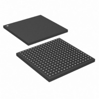
DS33X42+ Maxim Integrated Products, DS33X42+ Datasheet - Page 363

DS33X42+
Manufacturer Part Number
DS33X42+
Description
IC MAPPING ETHERNET 256CSBGA
Manufacturer
Maxim Integrated Products
Datasheet
1.DS33X11.pdf
(375 pages)
Specifications of DS33X42+
Applications
Data Transport
Interface
Parallel/Serial
Voltage - Supply
1.8V, 2.5V, 3.3V
Package / Case
256-CSBGA
Mounting Type
Surface Mount
Lead Free Status / RoHS Status
Lead free / RoHS Compliant
- Current page: 363 of 375
- Download datasheet (3Mb)
13.
The device supports the standard instruction codes SAMPLE:PRELOAD, BYPASS, and EXTEST. Optional public
instructions included are HIGHZ, CLAMP, and IDCODE. See
required by IEEE 1149.1 Standard Test Access Port and Boundary Scan Architecture.
The Test Access Port has the necessary interface pins; JTRST, JTCLK, JTMS, JTDI, and JTDO. See the pin
descriptions for details. Refer to IEEE 1149.1-1990, IEEE 1149.1a-1993, and IEEE 1149.1b-1994 for details about
the Boundary Scan Architecture and the Test Access Port.
Figure 13-1. JTAG Functional Block Diagram
Rev: 063008
________________________________________________ DS33X162/X161/X82/X81/X42/X41/X11/W41/W11
JTAG Information
10k Ω
Test Access Port (TAP)
TAP Controller
Instruction Register
V
DD
JTDI
10k Ω
V
DD
JTMS
TEST ACCESS PORT
BOUNDRY SCAN
IDENTIFICATION
CONTROLLER
INSTRUCTION
REGISTER
REGISTER
REGISTER
REGISTER
BYPASS
JTCLK
10k Ω
V
DD
JTRST
Bypass Register
Boundary Scan Register
Device Identification Register
Table
SELECT
TRI-STATE
13-1. The device contains the following as
MUX
JTDO
363 of 375
Related parts for DS33X42+
Image
Part Number
Description
Manufacturer
Datasheet
Request
R

Part Number:
Description:
MAX7528KCWPMaxim Integrated Products [CMOS Dual 8-Bit Buffered Multiplying DACs]
Manufacturer:
Maxim Integrated Products
Datasheet:

Part Number:
Description:
Single +5V, fully integrated, 1.25Gbps laser diode driver.
Manufacturer:
Maxim Integrated Products
Datasheet:

Part Number:
Description:
Single +5V, fully integrated, 155Mbps laser diode driver.
Manufacturer:
Maxim Integrated Products
Datasheet:

Part Number:
Description:
VRD11/VRD10, K8 Rev F 2/3/4-Phase PWM Controllers with Integrated Dual MOSFET Drivers
Manufacturer:
Maxim Integrated Products
Datasheet:

Part Number:
Description:
Highly Integrated Level 2 SMBus Battery Chargers
Manufacturer:
Maxim Integrated Products
Datasheet:

Part Number:
Description:
Current Monitor and Accumulator with Integrated Sense Resistor; ; Temperature Range: -40°C to +85°C
Manufacturer:
Maxim Integrated Products

Part Number:
Description:
TSSOP 14/A�/RS-485 Transceivers with Integrated 100O/120O Termination Resis
Manufacturer:
Maxim Integrated Products

Part Number:
Description:
TSSOP 14/A�/RS-485 Transceivers with Integrated 100O/120O Termination Resis
Manufacturer:
Maxim Integrated Products

Part Number:
Description:
QFN 16/A�/AC-DC and DC-DC Peak-Current-Mode Converters with Integrated Step
Manufacturer:
Maxim Integrated Products

Part Number:
Description:
TDFN/A/65V, 1A, 600KHZ, SYNCHRONOUS STEP-DOWN REGULATOR WITH INTEGRATED SWI
Manufacturer:
Maxim Integrated Products

Part Number:
Description:
Integrated Temperature Controller f
Manufacturer:
Maxim Integrated Products

Part Number:
Description:
SOT23-6/I�/45MHz to 650MHz, Integrated IF VCOs with Differential Output
Manufacturer:
Maxim Integrated Products

Part Number:
Description:
SOT23-6/I�/45MHz to 650MHz, Integrated IF VCOs with Differential Output
Manufacturer:
Maxim Integrated Products

Part Number:
Description:
EVALUATION KIT/2.4GHZ TO 2.5GHZ 802.11G/B RF TRANSCEIVER WITH INTEGRATED PA
Manufacturer:
Maxim Integrated Products

Part Number:
Description:
QFN/E/DUAL PCIE/SATA HIGH SPEED SWITCH WITH INTEGRATED BIAS RESISTOR
Manufacturer:
Maxim Integrated Products
Datasheet:


