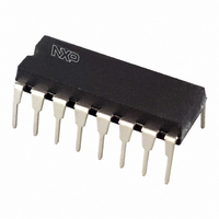
HEF4052BP,652 NXP Semiconductors, HEF4052BP,652 Datasheet - Page 6

HEF4052BP,652
Manufacturer Part Number
HEF4052BP,652
Description
IC MUX/DEMUX DUAL 4X1 16DIP
Manufacturer
NXP Semiconductors
Series
4000Br
Type
Analog Multiplexerr
Specifications of HEF4052BP,652
Package / Case
16-DIP (0.300", 7.62mm)
Function
Multiplexer/Demultiplexer
Circuit
2 x 4:1
On-state Resistance
175 Ohm
Voltage Supply Source
Single Supply
Voltage - Supply, Single/dual (±)
3 V ~ 15 V, -18 V ~ 0.5 V
Operating Temperature
-40°C ~ 85°C
Mounting Type
Through Hole
Number Of Channels
2 Channel
On Resistance (max)
2500 Ohm @ 5 V
On Time (max)
260 ns @ 5 V
Off Time (max)
205 ns @ 5 V
Supply Voltage (max)
15.5 V
Supply Voltage (min)
4.5 V
Mounting Style
Through Hole
Number Of Switches
Dual
Package
16PDIP
Maximum On Resistance
2500@5V Ohm
Maximum Propagation Delay Bus To Bus
305@5V|150@10V|100@15V ns
Maximum Low Level Output Current
10 mA
Multiplexer Architecture
4:1
Maximum Turn-off Time
205@5V ns
Maximum Turn-on Time
260@5V ns
Power Supply Type
Single
Lead Free Status / RoHS Status
Lead free / RoHS Compliant
Lead Free Status / RoHS Status
Lead free / RoHS Compliant, Lead free / RoHS Compliant
Other names
568-3109-5
933282430652
HEF4052BPN
933282430652
HEF4052BPN
NXP Semiconductors
7. Functional description
Table 3.
[1]
8. Limiting values
Table 4.
In accordance with the Absolute Maximum Rating System (IEC 60134). Voltages are referenced to V
[1]
[2]
HEF4052B_7
Product data sheet
Input
E
L
L
L
L
H
Symbol
V
V
I
V
I
I
T
T
P
P
IK
I/O
DD
stg
amb
DD
EE
I
tot
H = HIGH voltage level;
L = LOW voltage level;
X = don’t care.
To avoid drawing V
switch must not exceed 0.4 V. If the switch current flows into terminal Z, no V
is no limit for the voltage drop across the switch, but the voltages at Y and Z may not exceed V
For DIP16 package: P
For SO16 package: P
For SSOP16 package: P
Function table
Limiting values
Parameter
supply voltage
supply voltage
input clamping current
input voltage
input/output current
supply current
storage temperature
ambient temperature
total power dissipation
power dissipation
7.1 Function table
DD
tot
current out of terminal Z, when switch current flows into terminals Y, the voltage drop across the bidirectional
tot
S2
L
L
H
H
X
derates linearly with 8 mW/K above 70 °C.
derates linearly with 12 mW/K above 70 °C.
tot
[1]
derates linearly with 5.5 mW/K above 60 °C.
All information provided in this document is subject to legal disclaimers.
Conditions
referenced to V
pins Sn and E;
V
T
per output
amb
I
DIP16 package
SO16 package
TSSOP16 package
< −0.5 V or V
S1
L
H
L
H
X
Rev. 07 — 26 March 2010
= −40 °C to +125 °C
DD
I
> V
DD
Dual 4-channel analog multiplexer/demultiplexer
+ 0.5 V
DD
current will flow out of terminals Y, and in this case there
Channel on
nY0 to nZ
nY1 to nZ
nY2 to nZ
nY3 to nZ
switches off
[1]
[2]
Min
−0.5
−18
-
−0.5
-
-
−65
−40
-
-
-
-
DD
or V
EE
.
Max
+18
+0.5
±10
V
±10
+150
+125
750
500
500
100
50
HEF4052B
DD
SS
+ 0.5
= 0 V (ground).
© NXP B.V. 2010. All rights reserved.
Unit
V
V
mA
V
mA
mA
°C
°C
mW
mW
mW
mW
6 of 22


