OM13001,598 NXP Semiconductors, OM13001,598 Datasheet - Page 33
OM13001,598
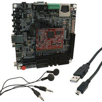
Manufacturer Part Number
OM13001,598
Description
EA LPC177X/8X EVAL BOARD
Manufacturer
NXP Semiconductors
Series
-r
Type
MCUr
Specifications of OM13001,598
Contents
Board, Cable, Headphones, Registration Card
Lead Free Status / Rohs Status
Lead free / RoHS Compliant
For Use With/related Products
LPC1788
Other names
568-6707


NXP Semiconductors
Table 3.
Not all functions are available on all parts. See
pins).
LPC178X_7X
Objective data sheet
Symbol
P4[29]
P4[30]
P4[31]
P5[0] to P5[4]
P5[0]
P5[1]
P5[2]
Pin description
176 B10
187 B7
193 A4
9
30
117 L14
F4
J4
…continued
B9
C7
E7
E5
H1
L12
122
130
134
6
21
81
[3]
[3]
[3]
[3]
[3]
[11]
All information provided in this document is subject to legal disclaimers.
I;
PU
I;
PU
I;
PU
I;
PU
I;
PU
<tb
d>
Table 2
Rev. 2 — 27 May 2011
I/O
O
I
O
I/O
O
O
O
I/O
O
I/O
O
I/O
I/O
I/O
I/O
O
I/O
I/O
I/O
O
I/O
-
-
O
-
I/O
(Ethernet, USB, LCD, QEI, SD/MMC, DAC pins) and
Description
P4[29] — General purpose digital input/output pin.
EMC_BLS3 — LOW active Byte Lane select signal 3.
U3_RXD — Receiver input for UART3.
T2_MAT1 — Match output for Timer 2, channel 1.
I2C2_SCL — I
specialized I2C pad).
LCD_VD[7] — LCD data.
LCD_VD[11] — LCD data.
LCD_VD[3] — LCD data.
P4[30] — General purpose digital input/output pin.
EMC_CS0 — LOW active Chip Select 0 signal.
P4[31] — General purpose digital input/output pin.
EMC_CS1 — LOW active Chip Select 1 signal.
Port 5: Port 5 is a 5-bit I/O port with individual direction controls
for each bit. The operation of port 5 pins depends upon the pin
function selected via the pin connect block.
P5[0] — General purpose digital input/output pin.
EMC_A[24] — External memory address line 24.
SSP2_MOSI — Master Out Slave In for SSP2.
T2_MAT2 — Match output for Timer 2, channel 2.
P5[1] — General purpose digital input/output pin.
EMC_A[25] — External memory address line 25.
SSP2_MISO — Master In Slave Out for SSP2.
T2_MAT3 — Match output for Timer 2, channel 3.
P5[2] — General purpose digital input/output pin.
R — Function reserved.
R — Function reserved.
T3_MAT2 — Match output for Timer 3, channel 2.
R — Function reserved.
I2C0_SDA — I
I
2
C pad that supports I
2
2
C2 clock input/output (this pin does not use a
C0 data input/output (this pin uses a specialized
32-bit ARM Cortex-M3 microcontroller
2
C Fast Mode Plus).
LPC178x/7x
© NXP B.V. 2011. All rights reserved.
Table 7
33 of 117
(EMC
Related parts for OM13001,598
Image
Part Number
Description
Manufacturer
Datasheet
Request
R

Part Number:
Description:
NXP Semiconductors designed the LPC2420/2460 microcontroller around a 16-bit/32-bitARM7TDMI-S CPU core with real-time debug interfaces that include both JTAG andembedded trace
Manufacturer:
NXP Semiconductors
Datasheet:

Part Number:
Description:
NXP Semiconductors designed the LPC2458 microcontroller around a 16-bit/32-bitARM7TDMI-S CPU core with real-time debug interfaces that include both JTAG andembedded trace
Manufacturer:
NXP Semiconductors
Datasheet:
Part Number:
Description:
NXP Semiconductors designed the LPC2468 microcontroller around a 16-bit/32-bitARM7TDMI-S CPU core with real-time debug interfaces that include both JTAG andembedded trace
Manufacturer:
NXP Semiconductors
Datasheet:
Part Number:
Description:
NXP Semiconductors designed the LPC2470 microcontroller, powered by theARM7TDMI-S core, to be a highly integrated microcontroller for a wide range ofapplications that require advanced communications and high quality graphic displays
Manufacturer:
NXP Semiconductors
Datasheet:
Part Number:
Description:
NXP Semiconductors designed the LPC2478 microcontroller, powered by theARM7TDMI-S core, to be a highly integrated microcontroller for a wide range ofapplications that require advanced communications and high quality graphic displays
Manufacturer:
NXP Semiconductors
Datasheet:
Part Number:
Description:
The Philips Semiconductors XA (eXtended Architecture) family of 16-bit single-chip microcontrollers is powerful enough to easily handle the requirements of high performance embedded applications, yet inexpensive enough to compete in the market for hi
Manufacturer:
NXP Semiconductors
Datasheet:
Part Number:
Description:
The XA-S3 device is a member of Philips Semiconductors? XA(eXtended Architecture) family of high performance 16-bitsingle-chip microcontrollers
Manufacturer:
NXP Semiconductors
Datasheet:

Part Number:
Description:
The NXP BlueStreak LH75401/LH75411 family consists of two low-cost 16/32-bit System-on-Chip (SoC) devices
Manufacturer:
NXP Semiconductors
Datasheet:
Part Number:
Description:
The NXP LPC3130/3131 combine an 180 MHz ARM926EJ-S CPU core, high-speed USB2
Manufacturer:
NXP Semiconductors
Datasheet:
Part Number:
Description:
The NXP LPC3141 combine a 270 MHz ARM926EJ-S CPU core, High-speed USB 2
Manufacturer:
NXP Semiconductors
Part Number:
Description:
The NXP LPC3143 combine a 270 MHz ARM926EJ-S CPU core, High-speed USB 2
Manufacturer:
NXP Semiconductors

Part Number:
Description:
The NXP LPC3152 combines an 180 MHz ARM926EJ-S CPU core, High-speed USB 2
Manufacturer:
NXP Semiconductors
Part Number:
Description:
The NXP LPC3154 combines an 180 MHz ARM926EJ-S CPU core, High-speed USB 2
Manufacturer:
NXP Semiconductors