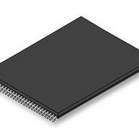
S29GL256S10TFI010 Spansion Inc., S29GL256S10TFI010 Datasheet - Page 29

S29GL256S10TFI010
Manufacturer Part Number
S29GL256S10TFI010
Description
Flash 256 MBIT 3V 100NS PAGE MODE FLASH
Manufacturer
Spansion Inc.
Datasheet
1.S29GL256S10TFI010.pdf
(97 pages)
Specifications of S29GL256S10TFI010
Data Bus Width
16 bit
Memory Type
Flash
Memory Size
256 Mbit
Architecture
Uniform
Timing Type
Asynchronous
Interface Type
CFI
Access Time
100 ns
Supply Voltage (max)
3.6 V
Supply Voltage (min)
2.7 V
Maximum Operating Current
100 mA
Operating Temperature
- 40 C to + 85 C
Mounting Style
SMD/SMT
Package / Case
TSOP-56
Lead Free Status / Rohs Status
Compliant
Available stocks
Company
Part Number
Manufacturer
Quantity
Price
Company:
Part Number:
S29GL256S10TFI010
Manufacturer:
Spansion
Quantity:
25
D a t a
S h e e t
( A d v a n c e
I n f o r m a t i o n )
other than the Program Buffer to Flash is written when that command is expected at the end of the word
count.
The write-buffer embedded programming operation can be suspended using the Program Suspend
command. When the Embedded Program algorithm is complete, the EAC then returns to the EAC standby or
Erase Suspend standby state where the programming operation was started.
The system can determine the status of the program operation by using Data Polling Status, reading the
Status Register, or monitoring the RY/BY# output. See
Status Register on page 38
for information on these
status bits. See
Data Polling Status on page 40
for information on these status bits. See
Figure 5.2
on page 30
for a diagram of the programming operation.
The Write Buffer Programming Sequence will be Aborted under the following conditions:
Load a Word Count value greater than the buffer size (255).
Write an address that is outside the Line provided in the Write to Buffer command.
The Program Buffer to Flash command is not issued after the Write Word Count number of data words is
loaded.
When any of the conditions that cause an abort of write buffer command occur the abort will happen
immediately after the offending condition, and will indicate a Program Fail in the Status Register at bit location
4 (PSB = 1) due to Write Buffer Abort bit location 3 (WBASB = 1). The next successful program operation will
clear the failure status or a Clear Status Register may be issued to clear the PSB status bit.
The Write Buffer Programming Sequence can be stopped by the following: Hardware Reset or Power cycle.
However, these using either of these methods may leave the area being programmed in an intermediate state
with invalid or unstable data values. In this case the same area will need to be reprogrammed with the same
data or erased to ensure data values are properly programmed or erased.
®
February 11, 2011 S29GL_128S_01GS_00_01
GL-S MirrorBit
Family
29


