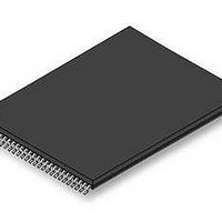
S29GL256S10TFI010 Spansion Inc., S29GL256S10TFI010 Datasheet - Page 43

S29GL256S10TFI010
Manufacturer Part Number
S29GL256S10TFI010
Description
Flash 256 MBIT 3V 100NS PAGE MODE FLASH
Manufacturer
Spansion Inc.
Datasheet
1.S29GL256S10TFI010.pdf
(97 pages)
Specifications of S29GL256S10TFI010
Data Bus Width
16 bit
Memory Type
Flash
Memory Size
256 Mbit
Architecture
Uniform
Timing Type
Asynchronous
Interface Type
CFI
Access Time
100 ns
Supply Voltage (max)
3.6 V
Supply Voltage (min)
2.7 V
Maximum Operating Current
100 mA
Operating Temperature
- 40 C to + 85 C
Mounting Style
SMD/SMT
Package / Case
TSOP-56
Lead Free Status / Rohs Status
Compliant
Available stocks
Company
Part Number
Manufacturer
Quantity
Price
Company:
Part Number:
S29GL256S10TFI010
Manufacturer:
Spansion
Quantity:
25
February 11, 2011 S29GL_128S_01GS_00_01
5.4.3.6
Notes:
1. Read toggle bit twice to determine whether or not it is toggling. See text.
2. Recheck toggle bit because it may stop toggling as DQ5 changes to 1. See text.
DQ5: Exceeded Timing Limits
DQ5 indicates whether the program or erase time has exceeded a specified internal pulse count limit. Under
these conditions DQ5 produces a '1'. This is a failure condition that indicates the program or erase cycle was
not successfully completed. The system must issue the reset command to return the device to reading array
data.
When a timeout occurs, the software must send a reset command to clear the timeout bit (DQ5) and to return
the EAC to read array mode. In this case, it is possible that the flash will continue to communicate busy for up
to 2 µs after the reset command is sent.
D a t a
S h e e t
( A d v a n c e
GL-S MirrorBit
Read DQ7 -DQ0 Twice (Notes 1, 2)
No
Figure 5.6 Toggle Bit Program
Read DQ7 -DQ0 (Note 1)
Read DQ7 -DQ0
Erase/Program
Operation Not
Complete
I n f o r m a t i o n )
Toggle Bit
= Toggle?
Toggle Bit
START
= Toggle?
DQ5 = 1?
®
Family
Yes
Yes
Yes
No
No
Operation Complete
Erase/Program
43


