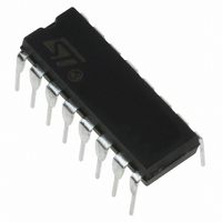
HCF4053BEY STMicroelectronics, HCF4053BEY Datasheet - Page 5

HCF4053BEY
Manufacturer Part Number
HCF4053BEY
Description
IC MUX/DEMUX TRIPLE 2X1 16DIP
Manufacturer
STMicroelectronics
Series
4000Br
Type
Analog Multiplexerr
Specifications of HCF4053BEY
Function
Multiplexer/Demultiplexer
Circuit
3 x 2:1
On-state Resistance
280 Ohm
Voltage Supply Source
Dual Supply
Voltage - Supply, Single/dual (±)
±3 V ~ 20 V
Current - Supply
.08µA
Operating Temperature
-55°C ~ 125°C
Mounting Type
Through Hole
Package / Case
16-DIP (0.300", 7.62mm)
Number Of Channels
3 Channel
On Resistance (max)
1050 Ohms
Propagation Delay Time
60 ns
On Time (max)
720 ns
Off Time (max)
450 ns
Supply Voltage (max)
20 V
Supply Voltage (min)
3 V
Maximum Power Dissipation
200 mW
Maximum Operating Temperature
+ 125 C
Minimum Operating Temperature
- 55 C
Mounting Style
Through Hole
Number Of Switches
3
Circuit Type
Monolithic Integrated
Current, Supply
3000 μA
Function Type
2-Channels, 3-Inputs
Logic Function
Multiplexer/Demultiplexer
Logic Type
MOS
Number Of Circuits
Triple
Package Type
DIP-16
Special Features
Binary
Temperature, Operating, Range
-55 to +125 °C
Voltage, Supply
3 to 20 V
Package
16PDIP
Maximum On Resistance
1050@5V Ohm
Maximum Propagation Delay Bus To Bus
60@5V|30@10V|20@15V ns
Multiplexer Architecture
2:1
Maximum Turn-off Time
450@5V ns
Maximum Turn-on Time
720@5V ns
Power Supply Type
Single
Multiplexer Configuration
Triple 2:1
Number Of Inputs
6
Number Of Outputs
3
Analog Switch On Resistance
1050@5VOhm
Analog Switch Turn On Time
720ns
Analog Switch Turn Off Time
450ns
Power Supply Requirement
Single
Single Supply Voltage (min)
3V
Single Supply Voltage (typ)
5/9/12/15/18V
Single Supply Voltage (max)
20V
Dual Supply Voltage (min)
Not RequiredV
Dual Supply Voltage (typ)
Not RequiredV
Dual Supply Voltage (max)
Not RequiredV
Power Dissipation
500mW
Mounting
Through Hole
Pin Count
16
Operating Temp Range
-55C to 125C
Operating Temperature Classification
Military
Lead Free Status / RoHS Status
Lead free / RoHS Compliant
Other names
497-1363-5
Available stocks
Company
Part Number
Manufacturer
Quantity
Price
Company:
Part Number:
HCF4053BEY
Manufacturer:
Dialight
Quantity:
40 000
Company:
Part Number:
HCF4053BEY
Manufacturer:
NXP
Quantity:
9 500
Part Number:
HCF4053BEY
Manufacturer:
ST
Quantity:
20 000
DYNAMIC ELECTRICAL CHARACTERISTICS (T
fall time = 20 ns )
(1 Both ends of channel.
* Peak to Peak voltage symmetrical about (V
Propagation Delay
Time (signal input to
output)
Frequency Response
Channel "ON" (sine
wave input) at
20 log V
Feed through (all
channels OFF) at
20 log V
Frequency Signal
Crosstalk at
20 log V
Sine Wave Distortion
f
CONTROL (Address or Inhibit)
Propagation Delay:
Address to Signal
OUT (Channels ON
or OFF)
Propagation Delay:
Inhibit to Signal OUT
(Channel turning ON)
Propagation Delay:
Inhibit to Signal OUT
(Channel turning
OFF)
Address or Inhibit to
Signal Crosstalk
IS
= 1KHz Sine Wave
Parameter
O
O
O
/V
/V
/V
I
I
I
= - 3dB
= - 40dB
= -40dB
= V
= V
= V
= V
V
-10
-10
(V)
-5
0
0
0
0
0
0
0
0
0
0
EE
SS
SS
SS
SS
10
(K )
200
R
10
10
1
1
1
1
L
(1)
DD
- V
(KHz)
EE
1
f
I
) /2
Test Condition
V
5(*)
5(*)
5(*)
2(*)
3(*)
5(*)
(V)
V
DD
I
amb
V
(V)
0
0
0
0
0
0
0
0
0
SS
= 25°C, C
V
(V)
10
15
10
10
10
10
15
10
15
10
15
10
15
10
5
5
5
5
5
5
5
5
DD
L
= 50pF, all input square wave rise and
V
OUT/IN
V
channel
V
OUT/IN
V
channel
Between any 2
Sections (IN pin
2, OUT pin 14)
Between any 2
Sections (lN pin
15, OUT pin 14)
V
(square wave)
O
O
O
O
C
at Common
at any
at Common
at any
= V
DD
-V
SS
Min. Typ. Max.
Value
0.12
360
160
120
225
360
160
120
200
200
130
2.5
0.3
0.2
30
15
11
25
60
10
90
70
65
8
6
HCF4053B
720
320
240
450
720
320
240
400
450
210
160
300
60
30
20
peak
MHz
MHz
MHz
Unit
mV
ns
ns
ns
ns
%
5/10


