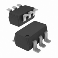
NX3L1T3157GW,125 NXP Semiconductors, NX3L1T3157GW,125 Datasheet - Page 11

NX3L1T3157GW,125
Manufacturer Part Number
NX3L1T3157GW,125
Description
IC SWITCH SPDT SC88
Manufacturer
NXP Semiconductors
Datasheet
1.NX3L1T3157GM115.pdf
(21 pages)
Specifications of NX3L1T3157GW,125
Package / Case
6-TSSOP, SC-88, SOT-363
Function
Switch
Circuit
1 x SPDT
On-state Resistance
500 mOhm
Voltage Supply Source
Single Supply
Voltage - Supply, Single/dual (±)
1.4 V ~ 4.3 V
Current - Supply
150nA
Operating Temperature
-40°C ~ 125°C
Mounting Type
Surface Mount
Switch Configuration
SPDT
On Resistance (max)
1.6 Ohm (Typ) @ 1.4 V
On Time (max)
90 ns @ 1.6 V
Off Time (max)
70 ns @ 1.6 V
Supply Voltage (max)
4.3 V
Supply Voltage (min)
1.4 V
Maximum Power Dissipation
250 mW
Maximum Operating Temperature
+ 125 C
Mounting Style
SMD/SMT
Minimum Operating Temperature
- 40 C
Lead Free Status / RoHS Status
Lead free / RoHS Compliant
Lead Free Status / RoHS Status
Lead free / RoHS Compliant, Lead free / RoHS Compliant
Other names
935287074125
NX3L1T3157GW-G
NX3L1T3157GW-G
NX3L1T3157GW-G
NX3L1T3157GW-G
Available stocks
Company
Part Number
Manufacturer
Quantity
Price
Company:
Part Number:
NX3L1T3157GW,125
Manufacturer:
NXP Semiconductors
Quantity:
4 700
NXP Semiconductors
Table 9.
At recommended operating conditions; voltages are referenced to GND (ground = 0 V); for load circuit see
[1]
[2]
Table 10.
NX3L1T3157_7
Product data sheet
Symbol Parameter
t
Supply voltage
V
1.4 V to 4.3 V
b-m
Fig 15. Enable and disable times
CC
Typical values are measured at T
Break-before-make guaranteed by design.
Measurement points are given in
Logic level: V
break-before-make
time
Dynamic characteristics
Measurement points
12.1 Waveform and test circuits
Y1 connected to V
Y0 connected to V
OH
is typical output voltage level that occurs with the output load.
Conditions
see
EXT
EXT
V
V
V
V
V
amb
CC
CC
CC
CC
CC
Figure 16
= 25 °C and V
…continued
= 1.4 V to 1.6 V
= 1.65 V to 1.95 V
= 2.3 V to 2.7 V
= 2.7 V to 3.6 V
= 3.6 V to 4.3 V
OFF to HIGH
HIGH to OFF
HIGH to OFF
OFF to HIGH
Table
Z output
Z output
S input
10.
Input
V
0.5V
Rev. 07 — 21 January 2010
GND
GND
GND
CC
M
V
V
OH
OH
V
= 1.5 V, 1.8 V, 2.5 V, 3.3 and 4.3 V respectively.
CC
I
[2]
t
V
dis
M
t
Low-ohmic single-pole double-throw analog switch
en
Min
V
X
-
-
-
-
-
V
X
25 °C
Typ
19
17
13
10
10
[1]
Max
-
-
-
-
-
t
Output
V
0.9V
V
dis
X
X
t
Min
en
9
7
4
3
2
OH
V
−40 °C to +125 °C
X
NX3L1T3157
001aag570
(85 °C)
Max
-
-
-
-
-
© NXP B.V. 2010. All rights reserved.
Figure
(125 °C)
Max
-
-
-
-
-
17.
11 of 21
Unit
ns
ns
ns
ns
ns


