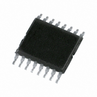
74HCT4053PW,118 NXP Semiconductors, 74HCT4053PW,118 Datasheet - Page 11

74HCT4053PW,118
Manufacturer Part Number
74HCT4053PW,118
Description
IC MUX/DEMUX TRIPLE 2X1 16TSSOP
Manufacturer
NXP Semiconductors
Series
74HCTr
Datasheet
1.74HC4053D653.pdf
(32 pages)
Specifications of 74HCT4053PW,118
Package / Case
16-TSSOP (0.173", 4.40mm Width)
Function
Multiplexer/Demultiplexer
Circuit
3 x 2:1
On-state Resistance
60 Ohm
Voltage Supply Source
Dual Supply
Voltage - Supply, Single/dual (±)
±4.5 V ~ 5.5 V
Current - Supply
50µA
Operating Temperature
-40°C ~ 125°C
Mounting Type
Surface Mount
Number Of Channels
3 Channel
On Resistance (max)
180 Ohm @ 4.5 V
On Time (max)
48 ns @ 4.5 V
Off Time (max)
44 ns @ 4.5 V
Supply Voltage (max)
5.5 V
Supply Voltage (min)
4.5 V
Maximum Power Dissipation
500 mW
Maximum Operating Temperature
+ 125 C
Minimum Operating Temperature
- 40 C
Mounting Style
SMD/SMT
Number Of Switches
Triple
Lead Free Status / RoHS Status
Lead free / RoHS Compliant
Lead Free Status / RoHS Status
Lead free / RoHS Compliant, Lead free / RoHS Compliant
Other names
568-4483-2
74HCT4053PW-T
74HCT4053PW-T
935188480118
74HCT4053PW-T
74HCT4053PW-T
935188480118
NXP Semiconductors
Table 7.
Voltages are referenced to GND (ground = 0 V).
V
V
Table 8.
Voltages are referenced to GND (ground = 0 V).
V
V
74HC_HCT4053
Product data sheet
Symbol
I
I
I
I
Symbol
T
V
V
I
I
I
I
ΔI
C
C
I
S(OFF)
S(ON)
CC
I
S(OFF)
S(ON)
CC
is
os
is
os
amb
IH
IL
I
sw
CC
is the input voltage at pins nYn or nZ, whichever is assigned as an input.
is the input voltage at pins nYn or nZ, whichever is assigned as an input.
is the output voltage at pins nZ or nYn, whichever is assigned as an output.
is the output voltage at pins nZ or nYn, whichever is assigned as an output.
= 25 °C
Static characteristics for 74HC4053
Static characteristics for 74HCT4053
Parameter
input leakage current
OFF-state leakage
current
ON-state leakage
current
supply current
Parameter
HIGH-level input
voltage
LOW-level input
voltage
input leakage current
OFF-state leakage
current
ON-state leakage
current
supply current
additional supply
current
input capacitance
switch capacitance
Conditions
V
V
|V
V
V
V
V
Conditions
V
V
V
V
|V
V
|V
V
V
per input; V
or GND; V
independent pins nYn
common pins nZ
EE
CC
I
CC
EE
os
CC
CC
I
CC
CC
I
os
SW
SW
SW
V
V
per channel
all channels
V
V
per channel
all channels
V
V
= V
= V
= V
CC
CC
CC
CC
CC
CC
= V
= V
All information provided in this document is subject to legal disclaimers.
= 0 V; V
= 0 V; V
= 10.0 V; V
= 10.0 V; V
= 4.5 V to 5.5 V
= 4.5 V to 5.5 V
= 10.0 V; V
= 10.0 V; V
| = V
| = V
| = V
IH
CC
CC
= 6.0 V
= 10.0 V
= 6.0 V
= 10.0 V
= 5.5 V; V
= 5.0 V; V
CC
CC
or V
CC
or GND; V
CC
CC
or GND; V
CC
or V
or V
I
Rev. 5 — 18 January 2011
…continued
− V
I
− V
− V
I
IL
= V
= V
= 4.5 V to 5.5 V; V
= V
; |V
EE
EE
EE
EE
EE
EE
EE
EE
EE
CC
CC
EE
EE
CC
SW
; see
; see
; see
= 0 V; V
= 0 V; see
= 0 V; V
= 0 V; V
− 2.1 V; other inputs at V
CC
is
= 0 V
= −5.0 V
| = V
or GND; V
or GND
= V
= 5.5 V; V
Figure 11
Figure 11
Figure 12
CC
EE
I
I
I
Triple 2-channel analog multiplexer/demultiplexer
− V
= V
= V
= V
or V
Figure 12
is
EE
IH
IH
IH
EE
CC
74HC4053; 74HCT4053
= V
EE
;
or V
or V
or V
;
= 0 V
= 0 V
EE
IL
IL
IL
or V
;
;
;
CC
CC
;
Min
-
-
-
-
-
-
-
Min
2.0
-
-
-
-
-
-
-
-
-
-
-
-
Typ
-
-
-
-
-
-
Typ
1.6
1.2
-
-
-
-
-
-
50
3.5
5
8
© NXP B.V. 2011. All rights reserved.
Max
±1.0
±2.0
±1.0
±1.0
±1.0
160.0
320.0
Max
-
0.8
±0.1
±0.1
±0.1
±0.1
8.0
16.0
180
-
-
-
Unit
μA
μA
μA
μA
μA
μA
μA
Unit
V
V
μA
μA
μA
μA
μA
μA
μA
pF
pF
pF
11 of 32


