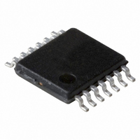
74HCT4066PW,118 NXP Semiconductors, 74HCT4066PW,118 Datasheet - Page 2

74HCT4066PW,118
Manufacturer Part Number
74HCT4066PW,118
Description
IC SWITCH QUAD 1X2 14TSSOP
Manufacturer
NXP Semiconductors
Series
74HCTr
Datasheet
1.74HC4066N652.pdf
(27 pages)
Specifications of 74HCT4066PW,118
Function
Switch
Circuit
4 x 1:1
Voltage Supply Source
Single Supply
Voltage - Supply, Single/dual (±)
4.5 V ~ 5.5 V
Current - Supply
40µA
Operating Temperature
-40°C ~ 125°C
Mounting Type
Surface Mount
Package / Case
14-TSSOP (0.173", 4.40mm Width)
Lead Free Status / RoHS Status
Lead free / RoHS Compliant
Other names
74HCT4066PW-T
74HCT4066PW-T
935187510118
74HCT4066PW-T
935187510118
Philips Semiconductors
FEATURES
QUICK REFERENCE DATA
GND = 0 V; T
Notes
1. C
2. For 74HC4066 the condition is V
2004 Nov 11
t
t
C
C
C
PZH
PHZ
Very low ON-resistance:
– 50
– 45
– 35
Complies with JEDEC standard no. 7A
ESD protection:
HBM EIA/JESD22-A114-B exceeds 2000 V
MM EIA/JESD22-A115-A exceeds 200 V.
Specified from 40 C to +85 C and 40 C to +125 C.
I
PD
S
Quad bilateral switches
SYMBOL
P
f
f
C
C
V
N = number of inputs switching;
For 74HCT4066 the condition is V
i
o
/t
/t
[(C
D
CC
PD
= input frequency in MHz;
L
S
PZL
PLZ
= output frequency in MHz;
= output load capacitance in pF;
= C
= maximum switch capacitance in pF;
L
is used to determine the dynamic power dissipation (P
= supply voltage in V;
+ C
(typical) at V
(typical) at V
(typical) at V
PD
S
amb
)
V
turn-on time nE to V
turn-off time nE to V
input capacitance
power dissipation
capacitance per switch
maximum switch
capacitance
CC
= 25 C; t
V
CC
2
2
PARAMETER
f
CC
CC
CC
i
f
o
= 4.5 V
= 6.0 V
= 9.0 V.
N + [(C
] = sum of the outputs.
r
= t
f
= 6 ns.
L
os
os
I
+ C
= GND to V
I
= GND to V
S
)
C
C
notes 1 and 2
V
L
L
CC
= 15 pF; R
= 15 pF; R
2
CC
CC
.
f
o
] where:
CONDITIONS
1.5 V.
L
L
2
= 1 k ; V
= 1 k ; V
GENERAL DESCRIPTION
The 74HC4066 and 74HCT4066 are high-speed Si-gate
CMOS devices and are pin compatible with the
HEF4066B. They are specified in compliance with JEDEC
standard no. 7A.
The 74HC4066 and 74HCT4066 have four independent
analog switches. Each switch has two input/output pins
(pins nY or nZ) and an active HIGH enable input pin
(pin nE). When pin nE = LOW the belonging analog switch
is turned off.
The 74HC4066 and 74HCT4066 are pin compatible with
the 74HC4016 and 74HCT4016 but exhibit a much lower
on-resistance. In addition, the on-resistance is relatively
constant over the full input signal range.
D
in W).
CC
CC
= 5 V 11
= 5 V 13
74HC4066; 74HCT4066
3.5
11
8
74HC4066
TYPICAL
12
16
3.5
12
8
Product specification
74HCT4066
ns
ns
pF
pF
pF
UNIT


