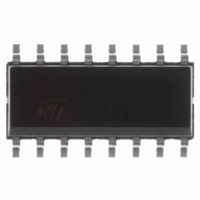
M74HC4051RM13TR STMicroelectronics, M74HC4051RM13TR Datasheet - Page 8

M74HC4051RM13TR
Manufacturer Part Number
M74HC4051RM13TR
Description
IC MUX/DEMUX 8X1 16SOIC
Manufacturer
STMicroelectronics
Series
74HCr
Type
Analog Multiplexerr
Datasheet
1.M74HC4051RM13TR.pdf
(17 pages)
Specifications of M74HC4051RM13TR
Function
Multiplexer/Demultiplexer
Circuit
1 x 8:1
On-state Resistance
100 Ohm
Voltage Supply Source
Dual Supply
Voltage - Supply, Single/dual (±)
±2 V ~ 6 V
Current - Supply
8µA
Operating Temperature
-55°C ~ 125°C
Mounting Type
Surface Mount
Package / Case
16-SOIC (0.154", 3.90mm Width)
Number Of Channels
1 Channel
On Resistance (max)
180 Ohms
Propagation Delay Time
60 ns
On Time (max)
225 ns
Off Time (max)
250 ns
Supply Voltage (max)
6 V
Supply Voltage (min)
2 V
Maximum Power Dissipation
500 mW
Maximum Operating Temperature
+ 125 C
Minimum Operating Temperature
- 55 C
Mounting Style
SMD/SMT
Number Of Switches
Single
No. Of Circuits
1
Supply Current
8µA
On State Resistance Max
50ohm
Supply Voltage Range
2V To 6V
Operating Temperature Range
-55°C To +125°C
Analogue Switch Case Style
SOP
No. Of Pins
16
Rohs Compliant
Yes
Multiplexer Configuration
Single 8:1
Number Of Inputs
8
Number Of Outputs
1
Analog Switch On Resistance
180@4.5VOhm
Analog Switch Turn On Time
225ns
Analog Switch Turn Off Time
250ns
Package Type
SOP
Power Supply Requirement
Single/Dual
Single Supply Voltage (min)
2V
Single Supply Voltage (typ)
3/5V
Single Supply Voltage (max)
6V
Dual Supply Voltage (min)
±1V
Dual Supply Voltage (typ)
±3/±5V
Dual Supply Voltage (max)
±6V
Power Dissipation
180mW
Mounting
Surface Mount
Pin Count
16
Operating Temp Range
-55C to 125C
Operating Temperature Classification
Military
Lead Free Status / RoHS Status
Lead free / RoHS Compliant
Other names
497-1846-2
Available stocks
Company
Part Number
Manufacturer
Quantity
Price
Company:
Part Number:
M74HC4051RM13TR
Manufacturer:
ST
Quantity:
12 000
Part Number:
M74HC4051RM13TR
Manufacturer:
ST
Quantity:
20 000
Maximum ratings
Table 9.
1. Input common terminal, and measured at switch terminal.
2. Input switch terminal, and measured at common terminal.
These characteristics are determined by the design of the device.
8/17
Symbo
f
f
MAX
MAX
l
Sine wave
distortion
Frequency
response
(Switch on)
Frequency
response
(switch on)
Feed through
attenuation
(switch off)
Crosstalk
(control input to
signal output)
Crosstalk
(between any
two switches)
Parameter
Analog switch characteristics (
(2)
(1)
2.25
2.25
2.25
2.25
2.25
2.25
V
(V)
4.5
6.0
4.5
6.0
4.5
6.0
4.5
6.0
4.5
6.0
4.5
6.0
CC
-2.25
-2.25
-2.25
-2.25
-2.25
-2.25
V
-4.5
-6.0
-4.5
-6.0
-4.5
-6.0
-4.5
-6.0
-4.5
-6.0
-4.5
-6.0
(V)
EE
Adjust f
Increase f
R
Adjust f
Increase f
R
V
Adjust input for 0 dBm
R
Adjust R
R
Adjust V
R
(V
V
IN
L
L
L
L
L
11
p-p
4
8
IN
= 50
= 50
= 600
= 600
= 600
is centered at (V
)
GND = 0 V; T
IN
IN
Ω
Ω
IN
L
, C
, C
Ω
Ω
IN
IN
voltage to obtain 0 dBm at V
voltage to obtain 0 dBm at V
at set up so that I
Ω
Test condition
, C
, C
to obtain 0d Bm at input
, C
L
f
Frequency until dB meter reads -3dB
L
Frequency until dB meter reads -3dB
IN
= 10 pF, f
L
L
= 10 pF, f
L
= 50 pF, f
= 50 pF, f
= 1 KHz R
= 50 pF, f
A
CC
= 25°C)
IN
IN
- V
IN
IN
= 1KHz sine wave
IN
= 1 KHz sine wave
L
EE
= 1 KHz sine wave
= 1 KHz square wave
= 10 K
S
= 1 KHz sine wave
)/2
= 0A.
Ω
C
L
OS
OS
= 50 pF
.
.
Value
0.025
0.020
0.018
Typ
120
190
200
140
200
-50
-50
-50
-50
-50
-50
45
70
85
60
M74HC4051
Unit
MHz
MHz
mV
dB
dB
%


