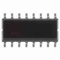
M74HCT4051RM13TR STMicroelectronics, M74HCT4051RM13TR Datasheet

M74HCT4051RM13TR
Specifications of M74HCT4051RM13TR
M74HCT4051RM13TR
Available stocks
Related parts for M74HCT4051RM13TR
M74HCT4051RM13TR Summary of contents
Page 1
... GND and C control inputs select one channel out of eight channels; they are compatible with TTL output level. 2 MOS technology All inputs are equipped with protection circuits against static discharge and transient excess voltage. M74HCT4051 SINGLE 8-CHANNEL DIP SOP TUBE T & R M74HCT4051B1R M74HCT4051M1R M74HCT4051RM13TR M74HCT4051TTR TSSOP 1/14 ...
Page 2
M74HCT4051 CONTROL INPUT EQUIVALENT CIRCUIT I/O EQUIVALENT CIRCUIT FUNCTIONAL DIAGRAM 2/14 PIN DESCRIPTION PIN No SYMBOL NAME AND FUNCTION 3 COM Common Output/Input OUT/IN 6 INH INHIBIT Input 7 V Negative Supply Voltage EE 11, 10 ...
Page 3
ABSOLUTE MAXIMUM RATINGS Symbol V Supply Voltage Supply Voltage Control Input Voltage I V Switch I/O Voltage I/O I Control Input Diode Current CK I I/O Diode Current IOK I Switch Through Current ...
Page 4
M74HCT4051 DC SPECIFICATIONS Symbol Parameter V CC (V) V High Level Input 4.5 IHC Voltage to 5.5 V Low Level Input 4.5 ILC Voltage to 5 Resistance 4.5 ON 4.5 4.5 4.5 R Difference of ON 4.5 ON ...
Page 5
AC ELECTRICAL CHARACTERISTICS (C Symbol Parameter V CC (V) Phase Difference 4.5 I/O Between Input and 4.5 Output t Output Enable 4.5 PZL Time t 4.5 PZH t Output Disable 4.5 PLZ Time t 4.5 PHZ CAPACITANCE CHARACTERISTICS Symbol Parameter ...
Page 6
M74HCT4051 ANALOG SWITCH CHARACTERISTICS (GND = 0V;T Symbol Parameter V CC (V) Sine Wave 2.25 Distortion 4.5 Sine Wave 2.25 Distortion 4.5 f Frequency 2.25 MAX Response 4.5 (Switch ON) (*) f Frequency 2.25 MAX Response 4.5 (Switch ON) (**) ...
Page 7
SWITCHING CARACTERISTICS TEST CIRCUIT BANDWIDTH AND FEEDTHROUGH ATTENUATION CROSSTALK (control to output) CROSSTALK BETWEEN ANY TWO SWITCHES M74HCT4051 7/14 ...
Page 8
M74HCT4051 SWITCHING CHARACTERISTICS WAVEFORM CHANNEL RESISTANCE (R ON) 8/14 I (Opr.) CC ...
Page 9
Plastic DIP-16 (0.25) MECHANICAL DATA mm. DIM. MIN. a1 0. 17. TYP MAX. MIN. 0.020 1.65 0.030 0.5 0.25 20 8.5 2.54 7.1 5.1 3.3 1.27 M74HCT4051 inch ...
Page 10
M74HCT4051 DIM. MIN 0 0. 9 3.8 G 4 10/14 SO-16 MECHANICAL DATA mm. TYP MAX. 1.75 0.2 1.65 0.46 0.25 ...
Page 11
TSSOP16 MECHANICAL DATA DIM. MIN 0.05 A2 0.8 b 0.19 c 0.09 D 4.9 E 6 0˚ PIN 1 IDENTIFICATION 1 mm. TYP MAX. 1.2 0.15 1 1.05 ...
Page 12
M74HCT4051 DIM. MIN 12 6.45 Bo 10.3 Ko 2.1 Po 3.9 P 7.9 12/14 Tape & Reel SO-16 MECHANICAL DATA mm. TYP MAX. 330 13.2 22.4 6.65 10.5 2.3 4.1 8.1 inch ...
Page 13
Tape & Reel TSSOP16 MECHANICAL DATA mm. DIM. MIN 12 6.7 Bo 5.3 Ko 1.6 Po 3.9 P 7.9 TYP MAX. MIN. 330 13.2 0.504 0.795 2.362 22.4 6.9 0.264 5.5 0.209 ...
Page 14
... No license is granted by implication or otherwise under any patent or patent rights of STMicroelectronics. Specifications mentioned in this publication are subject to change without notice. This publication supersedes and replaces all information previously supplied ...


