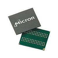
MT48LC4M32B2F5-6 Micron Technology Inc, MT48LC4M32B2F5-6 Datasheet - Page 27

MT48LC4M32B2F5-6
Manufacturer Part Number
MT48LC4M32B2F5-6
Description
Manufacturer
Micron Technology Inc
Type
SDRAMr
Datasheet
1.MT48LC4M32B2F5-6.pdf
(67 pages)
Specifications of MT48LC4M32B2F5-6
Organization
4Mx32
Density
128Mb
Address Bus
14b
Access Time (max)
17/7.5/5.5ns
Maximum Clock Rate
166MHz
Operating Supply Voltage (typ)
3.3V
Package Type
VFBGA
Operating Temp Range
0C to 70C
Operating Supply Voltage (max)
3.6V
Operating Supply Voltage (min)
3V
Supply Current
195mA
Pin Count
90
Mounting
Surface Mount
Operating Temperature Classification
Commercial
Lead Free Status / Rohs Status
Not Compliant
Available stocks
Company
Part Number
Manufacturer
Quantity
Price
Company:
Part Number:
MT48LC4M32B2F5-6:G
Manufacturer:
Micron Technology Inc
Quantity:
10 000
Company:
Part Number:
MT48LC4M32B2F5-6:G TR
Manufacturer:
Micron Technology Inc
Quantity:
10 000
Company:
Part Number:
MT48LC4M32B2F5-6AIT:L
Manufacturer:
MICRON
Quantity:
1 000
Figure 15:
PDF: 09005aef80872800/Source: 09005aef80863355
128MbSDRAMx32_2.fm - Rev. L 1/09 EN
Terminating a READ Burst
Notes:
tage of the PRECHARGE command is that it requires that the command and address
buses be available at the appropriate time to issue the command; the advantage of the
PRECHARGE command is that it can be used to truncate fixed-length or full-page bursts.
Full-page READ bursts can be truncated with the BURST TERMINATE command, and
fixed-length READ bursts may be truncated with a BURST TERMINATE command,
provided that auto precharge was not activated. The BURST TERMINATE command
should be issued x cycles before the clock edge at which the last desired data element is
valid, where x = CL - 1. This is shown in Figure 15 for each possible CL; data element n +
3 is the last desired data element of a longer burst.
COMMAND
COMMAND
1. DQM is LOW.
COMMAND
ADDRESS
ADDRESS
ADDRESS
CLK
CLK
CLK
DQ
DQ
DQ
BANK,
BANK,
COL n
COL n
T0
T0
T0
BANK,
COL n
READ
READ
READ
CL = 1
CL = 2
T1
T1
T1
NOP
NOP
NOP
D
CL = 3
OUT
n
T2
T2
T2
NOP
NOP
NOP
D
D
n + 1
OUT
OUT
n
27
T3
T3
T3
NOP
NOP
NOP
D
n + 2
D
D
n + 1
OUT
OUT
OUT
n
TERMINATE
TERMINATE
TERMINATE
Micron Technology, Inc., reserves the right to change products or specifications without notice.
BURST
BURST
BURST
T4
T4
T4
X = 0 cycles
X = 1 cycle
D
n + 2
D
n + 3
D
n + 1
OUT
OUT
OUT
X = 2 cycles
T5
T5
T5
NOP
NOP
NOP
D
n + 3
D
n + 2
OUT
OUT
T6
T6
T6
NOP
NOP
NOP
D
n + 3
OUT
DON’T CARE
T7
NOP
©2001 Micron Technology, Inc. All rights reserved.
128Mb: x32 SDRAM
Register Definition


