74AHC1G32GW NXP Semiconductors, 74AHC1G32GW Datasheet
74AHC1G32GW
Specifications of 74AHC1G32GW
Available stocks


Related parts for 74AHC1G32GW


74AHC1G32GW Summary of contents
Page 1
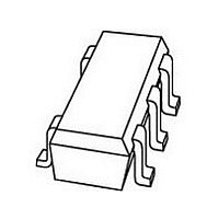
... Balanced propagation delays I SOT353-1 and SOT753 package options I Specified from +125 C 3. Ordering information Table 1. Ordering information Type number Package Temperature range 74AHC1G32GW +125 C 74AHCT1G32GW 74AHC1G32GV +125 C 74AHCT1G32GV Name Description TSSOP5 plastic thin shrink small outline package; 5 leads; body width 1.25 mm SC-74A plastic surface-mounted package ...
Page 2
... NXP Semiconductors 4. Marking Table 2. Marking codes Type number 74AHC1G32GW 74AHCT1G32GW 74AHC1G32GV 74AHCT1G32GV 5. Functional diagram Fig 1. Logic symbol Fig 3. Logic diagram 6. Pinning information 6.1 Pinning Fig 4. Pin configuration SOT353-1 (TSSOP5) and SOT753 (SC-74A) 74AHC_AHCT1G32_7 Product data sheet 74AHC1G32; 74AHCT1G32 Marking code ...
Page 3
... NXP Semiconductors 6.2 Pin description Table 3. Pin description Symbol Pin GND Functional description Table 4. Function table H = HIGH voltage level LOW voltage level Inputs Limiting values Table 5. Limiting values In accordance with the Absolute Maximum Rating System (IEC 60134). Symbol Parameter V supply voltage ...
Page 4
... NXP Semiconductors 9. Recommended operating conditions Table 6. Recommended operating conditions Voltages are referenced to GND (ground = 0 V). Symbol Parameter V supply voltage CC V input voltage I V output voltage O T ambient temperature amb t/ V input transition rise and fall rate 10. Static characteristics Table 7. Static characteristics Voltages are referenced to GND (ground = 0 V) ...
Page 5
... NXP Semiconductors Table 7. Static characteristics Voltages are referenced to GND (ground = 0 V). Symbol Parameter Conditions For type 74AHCT1G32 V HIGH-level input voltage V LOW-level input voltage V HIGH-level output voltage 8 LOW-level output voltage 8 input leakage GND current 5 supply current 5 additional per input pin; V ...
Page 6
... NXP Semiconductors Table 8. Dynamic characteristics GND = 3.0 ns. For waveform see r f Symbol Parameter Conditions For type 74AHCT1G32 t propagation A and delay see Figure power per buffer; PD dissipation pF MHz; L capacitance V = GND [ the same as t and PLH PHL [2] Typical values are measured at V [3] ...
Page 7
... NXP Semiconductors Test data is given in Table Definitions for test circuit Load capacitance including jig and probe capacitance Termination resistance should be equal to output impedance Z T Fig 6. Load circuitry for switching times 74AHC_AHCT1G32_7 Product data sheet 74AHC1G32; 74AHCT1G32 PULSE DUT GENERATOR Rev. 07 — 14 May 2009 ...
Page 8
... NXP Semiconductors 13. Package outline TSSOP5: plastic thin shrink small outline package; 5 leads; body width 1. DIMENSIONS (mm are the original dimensions UNIT max. 0.1 1.0 mm 1.1 0.15 0 0.8 Note 1. Plastic or metal protrusions of 0.15 mm maximum per side are not included. OUTLINE VERSION IEC SOT353-1 Fig 7 ...
Page 9
... NXP Semiconductors Plastic surface-mounted package; 5 leads DIMENSIONS (mm are the original dimensions UNIT 0.100 0.40 1.1 0.26 mm 0.013 0.25 0.9 0.10 OUTLINE VERSION IEC SOT753 Fig 8. Package outline SOT753 (SC-74A) 74AHC_AHCT1G32_7 Product data sheet 74AHC1G32; 74AHCT1G32 scale 3.1 1.7 3.0 0.6 0.95 2 ...
Page 10
... NXP Semiconductors 14. Abbreviations Table 10. Abbreviations Acronym Description CDM Charged Device Model DUT Device Under Test ESD ElectroStatic Discharge HBM Human Body Model MM Machine Model TTL Transistor-Transistor Logic 15. Revision history Table 11. Revision history Document ID Release date 74AHC_AHCT1G32_7 20090514 • Modifications: Pin configuration SOT353-1 (TSSOP5) and SOT753 (SC-74A) drawing corrected. ...
Page 11
... Right to make changes — NXP Semiconductors reserves the right to make changes to information published in this document, including without limitation specifications and product descriptions, at any time and without notice ...
Page 12
... NXP Semiconductors 18. Contents 1 General description . . . . . . . . . . . . . . . . . . . . . . 1 2 Features . . . . . . . . . . . . . . . . . . . . . . . . . . . . . . . 1 3 Ordering information . . . . . . . . . . . . . . . . . . . . . 1 4 Marking . . . . . . . . . . . . . . . . . . . . . . . . . . . . . . . . 2 5 Functional diagram . . . . . . . . . . . . . . . . . . . . . . 2 6 Pinning information . . . . . . . . . . . . . . . . . . . . . . 2 6.1 Pinning . . . . . . . . . . . . . . . . . . . . . . . . . . . . . . . 2 6.2 Pin description . . . . . . . . . . . . . . . . . . . . . . . . . 3 7 Functional description . . . . . . . . . . . . . . . . . . . 3 8 Limiting values Recommended operating conditions Static characteristics Dynamic characteristics . . . . . . . . . . . . . . . . . . 5 12 Waveforms . . . . . . . . . . . . . . . . . . . . . . . . . . . . . 6 13 Package outline . . . . . . . . . . . . . . . . . . . . . . . . . 8 14 Abbreviations ...