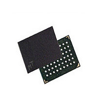
MT48LC8M16LFB4-8 Micron Technology Inc, MT48LC8M16LFB4-8 Datasheet - Page 36

MT48LC8M16LFB4-8
Manufacturer Part Number
MT48LC8M16LFB4-8
Description
Manufacturer
Micron Technology Inc
Type
Mobile SDRAMr
Datasheet
1.MT48LC8M16LFB4-8.pdf
(79 pages)
Specifications of MT48LC8M16LFB4-8
Organization
8Mx16
Density
128Mb
Address Bus
14b
Access Time (max)
19/8/7ns
Maximum Clock Rate
125MHz
Operating Supply Voltage (typ)
3.3V
Package Type
VFBGA
Operating Temp Range
0C to 70C
Operating Supply Voltage (max)
3.6V
Operating Supply Voltage (min)
3V
Supply Current
100mA
Pin Count
54
Mounting
Surface Mount
Operating Temperature Classification
Commercial
Lead Free Status / Rohs Status
Compliant
Available stocks
Company
Part Number
Manufacturer
Quantity
Price
Company:
Part Number:
MT48LC8M16LFB4-8 IT:G
Manufacturer:
Micron Technology Inc
Quantity:
10 000
Company:
Part Number:
MT48LC8M16LFB4-8 IT:G TR
Manufacturer:
Micron Technology Inc
Quantity:
10 000
Company:
Part Number:
MT48LC8M16LFB4-8 XT:G
Manufacturer:
Micron Technology Inc
Quantity:
10 000
Company:
Part Number:
MT48LC8M16LFB4-8:G
Manufacturer:
Micron Technology Inc
Quantity:
10 000
Company:
Part Number:
MT48LC8M16LFB4-8:G TR
Manufacturer:
Micron Technology Inc
Quantity:
10 000
Figure 23:
Figure 24:
PDF: 09005aef807f4885/Source: 09005aef8071a76b
128Mbx16x32Mobile_2.fm - Rev. L 10/07 EN
Random WRITE Cycles
WRITE-to-READ
Notes:
Notes:
In the case of a fixed-length burst being executed to completion, a PRECHARGE
command issued at the optimum time (as described above) provides the same operation
that would result from the same fixed-length burst with auto precharge. The disadvan-
tage of the PRECHARGE command is that it requires that the command and address
buses be available at the appropriate time to issue the command; the advantage of the
PRECHARGE command is that it can be used to truncate fixed-length or full-page bursts.
COMMAND
1. Each WRITE command may be to any bank.
2. DQM is LOW.
3. Example shows BL = 1 or an interrupting BL > 1.
COMMAND
1. The WRITE command may be to any bank, and the READ command may be to any bank.
2. DQM is LOW.
3. CL = 2 for illustration.
4. Data n + 1 is either the last data of BL = 1 or the last desired of a longer burst.
ADDRESS
ADDRESS
CLK
DQ
CLK
DQ
WRITE
BANK,
TRANSITIONING DATA
COL n
D
T0
BANK,
WRITE
COL n
n
IN
D
T0
n
IN
n + 1
NOP
T1
D
WRITE
BANK,
COL a
IN
T1
D
a
IN
TRANSITIONING DATA
BANK,
READ
COL b
T2
WRITE
BANK,
COL x
D
T2
36
x
IN
DON’T CARE
T3
NOP
WRITE
BANK,
COL m
T3
D
m
IN
Micron Technology, Inc., reserves the right to change products or specifications without notice.
NOP
D
T4
OUT
b
128Mb: x16, x32 Mobile SDRAM
DON’T CARE
NOP
T5
b + 1
D
OUT
©2001 Micron Technology, Inc. All rights reserved.
READs


