74ABT574AN NXP Semiconductors, 74ABT574AN Datasheet - Page 2
74ABT574AN
Manufacturer Part Number
74ABT574AN
Description
Flip Flops OCTAL D 3-S
Manufacturer
NXP Semiconductors
Datasheet
1.74ABT574AN.pdf
(11 pages)
Specifications of 74ABT574AN
Number Of Circuits
1
Logic Family
ABT
Logic Type
D-Type Edge Triggered Flip-Flop
Polarity
Non-Inverting
Input Type
Single-Ended
Propagation Delay Time
3.4 ns
High Level Output Current
- 32 mA
Supply Voltage (max)
5.5 V
Maximum Operating Temperature
+ 85 C
Mounting Style
Through Hole
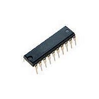
Package / Case
DIP-20
Minimum Operating Temperature
- 40 C
Supply Voltage (min)
4.5 V
Lead Free Status / Rohs Status
Details
Other names
74ABT574AN,112
Available stocks
Company
Part Number
Manufacturer
Quantity
Price


Philips Semiconductors
FEATURES
QUICK REFERENCE DATA
ORDERING INFORMATION
PIN CONFIGURATION
20-Pin Plastic DIP
20-Pin plastic SO
20-Pin Plastic SSOP Type II
20-Pin Plastic TSSOP Type I
1995 May 22
74ABT574A is flow-through pinout version of 74ABT374
Inputs and outputs on opposite side of package allow easy
interface to microprocessors
3-State outputs for bus interfacing
Power-up 3-State
Power-up reset
Common output enable
Latch-up protection exceeds 500mA per Jedec Std 17
ESD protection exceeds 2000 V per MIL STD 883 Method 3015
and 200 V per Machine Model
Live insertion/extraction permitted.
Octal D-type flip-flop (3-State)
SYMBOL
C
I
t
t
C
PLH
PHL
CCZ
OUT
IN
PACKAGES
GND
Propagation delay
CP to Qn
Input capacitance
Output capacitance
Total supply current
OE
D0
D1
D2
D3
D4
D5
D6
D7
10
1
2
3
4
5
6
7
8
9
PARAMETER
TEMPERATURE RANGE
20
19
18
17
16
15
14
13
12
11
–40 C to +85 C
–40 C to +85 C
–40 C to +85 C
–40 C to +85 C
V
Q0
Q1
Q2
Q3
Q4
Q5
Q6
Q7
CP
CC
SA00103
C
V
Outputs disabled; V
Outputs disabled; V
I
L
= 0V or V
= 50pF; V
OUTSIDE NORTH AMERICA
2
74ABT574A PW
74ABT574A DB
DESCRIPTION
The 74ABT574A high-performance BiCMOS device combines low
static and dynamic power dissipation with high speed and high
output drive.
The 74ABT574A is an 8-bit, edge triggered register coupled to eight
3-State output buffers. The two sections of the device are controlled
independently by the clock (CP) and Output Enable (OE) control
gates. The state of each D input (one set-up time before the
Low-to-High clock transition) is transferred to the corresponding
flip-flop’s Q output.
When OE is Low, the stored data appears at the outputs. When OE
is High, the outputs are in the High-impedance “off” state, which
means they will neither drive nor load the bus.
The 3-State output buffers are designed to drive heavily loaded
3-State buses, MOS memories, or MOS microprocessors. The
active-Low Output Enable (OE) controls all eight 3-State buffers
independent of the clock operation.
PIN DESCRIPTION
T
74ABT574A N
74ABT574A D
CC
amb
19, 18, 17,
16, 15, 14,
CC
NUMBER
2, 3, 4, 5,
6, 7, 8, 9
13, 12
CONDITIONS
PIN
= 5V
= 25 C; GND = 0V
11
10
20
1
O
CC
= 0V or V
=5.5V
SYMBOL
Q0-Q7
D0-D7
GND
V
OE
CP
CC
CC
NORTH AMERICA
7ABT574APW DH
74ABT574A DB
Output enable input (active-Low)
Data inputs
Data outputs
Clock pulse input (active rising edge)
Ground (0V)
Positive supply voltage
74ABT574A N
74ABT574A D
TYPICAL
FUNCTION
74ABT574A
100
3.0
3.4
3
6
Product specification
DWG NUMBER
853-1509 15261
SOT146-1
SOT163-1
SOT339-1
SOT360-1
UNIT
pF
pF
ns
A
Related parts for 74ABT574AN
Image
Part Number
Description
Manufacturer
Datasheet
Request
R

Part Number:
Description:
NXP Semiconductors designed the LPC2420/2460 microcontroller around a 16-bit/32-bitARM7TDMI-S CPU core with real-time debug interfaces that include both JTAG andembedded trace
Manufacturer:
NXP Semiconductors
Datasheet:

Part Number:
Description:
NXP Semiconductors designed the LPC2458 microcontroller around a 16-bit/32-bitARM7TDMI-S CPU core with real-time debug interfaces that include both JTAG andembedded trace
Manufacturer:
NXP Semiconductors
Datasheet:
Part Number:
Description:
NXP Semiconductors designed the LPC2468 microcontroller around a 16-bit/32-bitARM7TDMI-S CPU core with real-time debug interfaces that include both JTAG andembedded trace
Manufacturer:
NXP Semiconductors
Datasheet:
Part Number:
Description:
NXP Semiconductors designed the LPC2470 microcontroller, powered by theARM7TDMI-S core, to be a highly integrated microcontroller for a wide range ofapplications that require advanced communications and high quality graphic displays
Manufacturer:
NXP Semiconductors
Datasheet:
Part Number:
Description:
NXP Semiconductors designed the LPC2478 microcontroller, powered by theARM7TDMI-S core, to be a highly integrated microcontroller for a wide range ofapplications that require advanced communications and high quality graphic displays
Manufacturer:
NXP Semiconductors
Datasheet:
Part Number:
Description:
The Philips Semiconductors XA (eXtended Architecture) family of 16-bit single-chip microcontrollers is powerful enough to easily handle the requirements of high performance embedded applications, yet inexpensive enough to compete in the market for hi
Manufacturer:
NXP Semiconductors
Datasheet:
Part Number:
Description:
The XA-S3 device is a member of Philips Semiconductors? XA(eXtended Architecture) family of high performance 16-bitsingle-chip microcontrollers
Manufacturer:
NXP Semiconductors
Datasheet:

Part Number:
Description:
The NXP BlueStreak LH75401/LH75411 family consists of two low-cost 16/32-bit System-on-Chip (SoC) devices
Manufacturer:
NXP Semiconductors
Datasheet:
Part Number:
Description:
The NXP LPC3130/3131 combine an 180 MHz ARM926EJ-S CPU core, high-speed USB2
Manufacturer:
NXP Semiconductors
Datasheet:
Part Number:
Description:
The NXP LPC3141 combine a 270 MHz ARM926EJ-S CPU core, High-speed USB 2
Manufacturer:
NXP Semiconductors
Part Number:
Description:
The NXP LPC3143 combine a 270 MHz ARM926EJ-S CPU core, High-speed USB 2
Manufacturer:
NXP Semiconductors

Part Number:
Description:
The NXP LPC3152 combines an 180 MHz ARM926EJ-S CPU core, High-speed USB 2
Manufacturer:
NXP Semiconductors
Part Number:
Description:
The NXP LPC3154 combines an 180 MHz ARM926EJ-S CPU core, High-speed USB 2
Manufacturer:
NXP Semiconductors

Part Number:
Description:
Standard level N-channel enhancement mode Field-Effect Transistor (FET) in a plastic package using NXP High-Performance Automotive (HPA) TrenchMOS technology
Manufacturer:
NXP Semiconductors
Datasheet: