74LV132PW NXP Semiconductors, 74LV132PW Datasheet
74LV132PW
Specifications of 74LV132PW
Available stocks


Related parts for 74LV132PW


74LV132PW Summary of contents
Page 1
Quad 2-input NAND Schmitt trigger Rev. 05 — 2 July 2009 1. General description The 74LV132 is a low-voltage Si-gate CMOS device that is pin and function compatible with 74HC132 and 74HCT132. The 74LV132 contains four 2-input NAND gates ...
Page 2
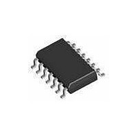
... NXP Semiconductors 4. Ordering information Table 1. Ordering information Type number Package Temperature range Name 74LV132N +125 C 74LV132D +125 C 74LV132DB +125 C 74LV132PW +125 C 74LV132BQ +125 C 5. Functional diagram mna407 Fig 1. Logic symbol 74LV132_5 Product data sheet Description DIP14 plastic dual in-line package; 14 leads (300 mil) SO14 plastic small outline package ...
Page 3
... NXP Semiconductors 6. Pinning information 6.1 Pinning 132 GND 001aac203 Fig 4. Pin configuration DIP14, SO14 and (T)SSOP14 6.2 Pin description Table 2. Pin description Symbol Pin GND 74LV132_5 Product data sheet (1) The die substrate is attached to the exposed die pad 3Y using conductive die attach material. It cannot be used as a supply pin or input. Fig 5. Pin confi ...
Page 4
... NXP Semiconductors 7. Functional description Table 3. Function table H = HIGH voltage level LOW voltage level. Input Limiting values Table 4. Limiting values In accordance with the Absolute Maximum Rating System (IEC 60134). Voltages are referenced to GND (ground = 0 V). Symbol Parameter V supply voltage CC I input clamping current ...
Page 5
... NXP Semiconductors 9. Recommended operating conditions Table 5. Recommended operating conditions Voltages are referenced to GND (ground = 0 V). Symbol Parameter [1] V supply voltage CC V input voltage I V output voltage O T ambient temperature amb [1] The static characteristics are guaranteed from 1.0 V (with input levels GND ...
Page 6
... NXP Semiconductors 11. Dynamic characteristics Table 7. Dynamic characteristics GND = 0 V; For test circuit see Figure Symbol Parameter Conditions t propagation delay nA nY; see power dissipation capacitance V = GND [1] All typical values are measured the same as t and PLH PHL [3] Typical values are measured at nominal supply voltage (V ...
Page 7
... NXP Semiconductors Table 8. Measurement points Supply voltage V CC < 2 3.6 V 4.5 V Test data is given in Table 9. Definitions test circuit Termination resistance should be equal to output impedance Load resistance Load capacitance including jig and probe capacitance. L Fig 7. Load circuit for switching times Table 9 ...
Page 8
... NXP Semiconductors Table 10. Transfer characteristics GND = 0 V; For test circuit see Figure Symbol Parameter Conditions V negative-going see T threshold voltage hysteresis voltage ( [1] All typical values are measured at T 14. Waveforms transfer characteristics Fig 8. Transfer characteristic 74LV132_5 Product data sheet …continued 7. Figure ...
Page 9
... NXP Semiconductors 0 Fig 10. Typical 74LV132 transfer characteristics Fig 12. Typical 74LV132 transfer characteristics 74LV132_5 Product data sheet 001aaa659 100 0.9 1.2 V (V) I Fig 11. Typical 74LV132 transfer characteristics 300 200 100 0 0 0.6 1.2 1.8 Rev. 05 — 2 July 2009 Quad 2-input NAND Schmitt trigger ...
Page 10
... NXP Semiconductors 15. Package outline DIP14: plastic dual in-line package; 14 leads (300 mil pin 1 index 1 DIMENSIONS (inch dimensions are derived from the original mm dimensions UNIT max. min. max. mm 4.2 0.51 3.2 inches 0.17 0.02 0.13 Note 1. Plastic or metal protrusions of 0.25 mm (0.01 inch) maximum per side are not included. ...
Page 11
... NXP Semiconductors SO14: plastic small outline package; 14 leads; body width 3 pin 1 index 1 e DIMENSIONS (inch dimensions are derived from the original mm dimensions) A UNIT max. 0.25 1.45 mm 1.75 0.25 0.10 1.25 0.010 0.057 inches 0.01 0.069 0.004 0.049 Note 1. Plastic or metal protrusions of 0.15 mm (0.006 inch) maximum per side are not included. ...
Page 12
... NXP Semiconductors SSOP14: plastic shrink small outline package; 14 leads; body width 5 pin 1 index 1 e DIMENSIONS (mm are the original dimensions) A UNIT max. 0.21 1. 0.25 0.05 1.65 Note 1. Plastic or metal protrusions of 0.25 mm maximum per side are not included. OUTLINE VERSION IEC SOT337-1 Fig 15. Package outline SOT337-1 (SSOP14) ...
Page 13
... NXP Semiconductors TSSOP14: plastic thin shrink small outline package; 14 leads; body width 4 pin 1 index 1 e DIMENSIONS (mm are the original dimensions) A UNIT max. 0.15 0.95 mm 1.1 0.25 0.05 0.80 Notes 1. Plastic or metal protrusions of 0.15 mm maximum per side are not included. 2. Plastic interlead protrusions of 0.25 mm maximum per side are not included. ...
Page 14
... NXP Semiconductors DHVQFN14: plastic dual in-line compatible thermal enhanced very thin quad flat package; no leads; 14 terminals; body 2 0.85 mm terminal 1 index area terminal 1 index area DIMENSIONS (mm are the original dimensions) (1) A UNIT max. 0.05 0. 0.2 0.00 0.18 Note 1. Plastic or metal protrusions of 0.075 mm maximum per side are not included. ...
Page 15
... NXP Semiconductors 16. Abbreviations Table 11. Abbreviations Acronym Description CMOS Complementary Metal Oxide Semiconductor DUT Device Under Test ESD ElectroStatic Discharge HBM Human Body Model MM Machine Model TTL Transistor-Transistor Logic 17. Revision history Table 12. Revision history Document ID Release date 74LV132_5 20090702 • Modifications: Table changed ...
Page 16
... Right to make changes — NXP Semiconductors reserves the right to make changes to information published in this document, including without limitation specifications and product descriptions, at any time and without notice ...
Page 17
... NXP Semiconductors 20. Contents 1 General description . . . . . . . . . . . . . . . . . . . . . . 1 2 Features . . . . . . . . . . . . . . . . . . . . . . . . . . . . . . . 1 3 Applications . . . . . . . . . . . . . . . . . . . . . . . . . . . . 1 4 Ordering information . . . . . . . . . . . . . . . . . . . . . 2 5 Functional diagram . . . . . . . . . . . . . . . . . . . . . . 2 6 Pinning information . . . . . . . . . . . . . . . . . . . . . . 3 6.1 Pinning . . . . . . . . . . . . . . . . . . . . . . . . . . . . . . . 3 6.2 Pin description . . . . . . . . . . . . . . . . . . . . . . . . . 3 7 Functional description . . . . . . . . . . . . . . . . . . . 4 8 Limiting values Recommended operating conditions Static characteristics Dynamic characteristics . . . . . . . . . . . . . . . . . . 6 12 Waveforms . . . . . . . . . . . . . . . . . . . . . . . . . . . . . 6 13 Transfer characteristics Waveforms transfer characteristics ...