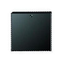
SC28L194A1A NXP Semiconductors, SC28L194A1A Datasheet - Page 42

SC28L194A1A
Manufacturer Part Number
SC28L194A1A
Description
UART Interface IC 3V-5V 4CH UART INTEL/MOT INTRF
Manufacturer
NXP Semiconductors
Type
Quad UART for 3.3 V and 5 V supply voltager
Datasheet
1.SC28L194A1BE.pdf
(52 pages)
Specifications of SC28L194A1A
Number Of Channels
4
Data Rate
460.8 Kbps
Supply Voltage (max)
5.5 V
Supply Voltage (min)
3 V
Supply Current
30 mA
Maximum Operating Temperature
+ 85 C
Minimum Operating Temperature
- 40 C
Package / Case
PLCC-68
Mounting Style
SMD/SMT
Operating Supply Voltage
3.3 V, 5 V
Lead Free Status / Rohs Status
Details
Other names
SC28L194A1A,512
Available stocks
Company
Part Number
Manufacturer
Quantity
Price
Company:
Part Number:
SC28L194A1A
Manufacturer:
NXP
Quantity:
5 530
Company:
Part Number:
SC28L194A1A
Manufacturer:
SEMTECH
Quantity:
384
Part Number:
SC28L194A1A
Manufacturer:
NXP/恩智浦
Quantity:
20 000
Company:
Part Number:
SC28L194A1A,512
Manufacturer:
NXP Semiconductors
Quantity:
10 000
1. Timing is illustrated and referenced with respect to W-RN and CEN inputs. Internal read and write activities are controlled by the Sclk as it
2. The minimum time before the rising edge of the next C2 time to stop the next bus cycle. CEN must return high after midpoint of C4 time and
3. Delay is from cEN high in Async mode to IRQN inactive, from end of C4 to IRQN inactive in sync mode.
4. The minimum frequency values are not tested, but are guaranteed by design.
5. 1MHz specification is for crystal operation.
Philips Semiconductors
AC ELECTRICAL SPECIFICATIONS FOR COMMERCIAL AND INDUSTRIAL (5V) (continued)
V
NOTES:
2006 Aug 15
Sclk Timing
X1/X2 Communication Crystal Clock
Counter/Timer Baud Rate Clock (External Clock Input)
DTACK Timing
I/O Port External Clock
Gout Timing
CC
SYMBOL
SYMBOL
Quad UART for 3.3 V and 5 V supply voltage
t
t
F
t/
Fx1
X1 L / H
T/RFx1
FC/T
TC/TLH
TC/TO
DAKdly
DAKdlya
DAKdlys
tgpirtx
GPOtdd
sclkl
sclkh
generates the several “C” timing as shown in the timing diagrams.
before the C2 time of the next cycle.
RFsck
sclk
= 5.0V
5
4
10%, –40 to +85 C
FIG #
FIG. #
Min low time at V
Min high time at V
Sclk frequency
Sclk rise and fall time (0.8 to 2.0 Volts)
X1 clock frequency
X1 Low / High time
X1 Rise and Fall time
Clock frequency
C/T high and low time
Delay C/T clock external to output pin
DACK low from Sclk C4 rising edge
DACK high from CEN high (Async)
DACK high from C4 end rising edge (Sync)
GPI to Rx/Tx clock out
RxD setup to I/OP rising edge 1X mode
I/OP falling edge to TxD out 1X mode
GPO valid after write to GPOR
IL
IH
(0.8V)
(2.0V)
PARAMETER
PARAMETER
42
MIN.
0.1
11
11
32
15
20
1
0
LIMITS
3.6864
TYP.
125
100
11
48
10
11
11
32
32
5
5
2
SC28L194
MAX.
Product data sheet
8.0
33
10
60
18
20
20
50
60
3
8
UNIT
UNIT
MHz
MHz
MHz
ns
ns
ns
ns
ns
ns
ns
ns
ns
ns
ns
ns
ns
ns


