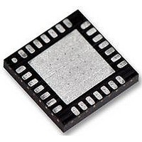
LM4836LQ National Semiconductor, LM4836LQ Datasheet - Page 19

LM4836LQ
Manufacturer Part Number
LM4836LQ
Description
34C6605
Manufacturer
National Semiconductor
Datasheet
1.LM4836LQNOPB.pdf
(28 pages)
Specifications of LM4836LQ
Amplifier Class
AB
No. Of Channels
2
Output Power
2.2W
Supply Voltage Range
2.7V To 5.5V
Load Impedance
3ohm
Operating Temperature Range
-40°C To +85°C
Amplifier Case Style
LLP
Rohs Compliant
No
Available stocks
Company
Part Number
Manufacturer
Quantity
Price
Part Number:
LM4836LQ
Manufacturer:
NS/国半
Quantity:
20 000
Application Information
the pop is directly proportional to the input capacitor’s size.
Higher value capacitors need more time to reach a quiescent
DC voltage (usually V
rent. The amplifier’s output charges the input capacitor
through the feedback resistor, R
mized by selecting an input capacitor value that is no higher
than necessary to meet the desired −3dB frequency.
A shown in Figure 1, the input resistor (20kΩ) and the input
capacitor produce a −3dB high pass filter cutoff frequency
that is found using Equation (7).
As an example when using a speaker with a low frequency
limit of 150Hz, the input coupling capacitor using Equation
(7), is 0.063µF. The 0.33µF input coupling capacitor shown
in Figure 1 allows the LM4835 to drive high efficiency, full
range speaker whose response extends below 30Hz.
OPTIMIZING CLICK AND POP REDUCTION
PERFORMANCE
The LM4836 contains circuitry that minimizes turn-on and
shutdown transients or “clicks and pop”. For this discussion,
turn-on refers to either applying the power supply voltage or
when the shutdown mode is deactivated. While the power
supply is ramping to its final value, the LM4836’s internal
amplifiers are configured as unity gain buffers. An internal
current source changes the voltage of the BYPASS pin in a
controlled, linear manner. Ideally, the input and outputs track
the voltage applied to the BYPASS pin. The gain of the
internal amplifiers remains unity until the voltage on the
bypass pin reaches 1/2 V
bypass pin is stable, the device becomes fully operational.
Although the BYPASS pin current cannot be modified,
changing the size of C
the magnitude of “clicks and pops”. Increasing the value of
C
presents a tradeoff: as the size of C
time increases. There is a linear relationship between the
size of C
turn-on times for various values of C
In order eliminate “clicks and pops”, all capacitors must be
discharged before turn-on. Rapidly switching V
allow the capacitors to fully discharge, which may cause
“clicks and pops”. In a single-ended configuration, the output
is coupled to the load by C
high value. C
Depending on the size of C
can be relatively large. To reduce transients in single-ended
B
reduces the magnitude of turn-on pops. However, this
B
and the turn-on time. Here are some typical
OUT
discharges through internal 20kΩ resistors.
C
DD
0.01µF
0.22µF
0.47µF
B
0.1µF
1.0µF
B
alters the device’s turn-on time and
/2) when charged with a fixed cur-
DD
OUT
OUT
. As soon as the voltage on the
. This capacitor usually has a
, the discharge time constant
f
. Thus, pops can be mini-
T
200ms
ON
B
20ms
44ms
94ms
B
2ms
increases, the turn-on
:
(Continued)
DD
may not
(7)
19
mode, an external 1kΩ–5kΩ resistor can be placed in par-
allel with the internal 20kΩ resistor. The tradeoff for using
this resistor is increased quiescent current.
DOCKING STATION
Applications such as notebook computers can take advan-
tage of a docking station to connect to external devices such
as monitors or audio/visual equipment that sends or receives
line level signals. The LM4836 has two outputs, Pin 9 and
Pin 13, which connect to outputs of the internal input ampli-
fiers that drive the volume control inputs. These input ampli-
fiers can drive loads of
with a rail-to-rail signal. Since the output signal present on
the RIGHT DOCK and LEFT DOCK pins is biased to V
coupling capacitors should be connected in series with the
load. Typical values for the coupling capacitors are 0.33µF to
1.0µF. If polarized coupling capacitors are used, connect
their "+" terminals to the respective output pin.
Since the DOCK outputs precede the internal volume con-
trol, the signal amplitude will be equal to the input signal’s
magnitude and cannot be adjusted. However, the input am-
plifier’s closed-loop gain can be adjusted using external
resistors. These resistors are shown in Figure 2 as 20kΩ
devices that set each input amplifier’s gain to -1. Use Equa-
tion 8 to determine the input and feedback resistor values for
a desired gain.
Adjusting the input amplifier’s gain sets the minimum gain for
that channel. The DOCK outputs adds circuit and functional
flexibility because their use supercedes using the inverting
outputs of each bridged output amplifier as line-level out-
puts.
STEREO-INPUT MULTIPLEXER (STEREO MUX)
The LM4836 has two stereo inputs. The MUX CONTROL pin
controls which stereo input is active. Applying 0V to the MUX
CONTROL pin selects stereo input 1. Applying V
MUX CONTROL pin selects stereo input 2.
BEEP DETECT FUNCTION
Computers and notebooks produce a system "beep" signal
that drives a small speaker. The speaker’s auditory output
signifies that the system requires user attention or input. To
FIGURE 2. Resistor for Varying Output Loads
- A
>
1kΩ (such as powered speakers)
v
= R
F
/ R
i
10108805
www.national.com
DD
to the
DD
(8)
/2,


