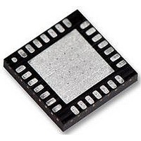
LM4836LQ National Semiconductor, LM4836LQ Datasheet - Page 22

LM4836LQ
Manufacturer Part Number
LM4836LQ
Description
34C6605
Manufacturer
National Semiconductor
Datasheet
1.LM4836LQNOPB.pdf
(28 pages)
Specifications of LM4836LQ
Amplifier Class
AB
No. Of Channels
2
Output Power
2.2W
Supply Voltage Range
2.7V To 5.5V
Load Impedance
3ohm
Operating Temperature Range
-40°C To +85°C
Amplifier Case Style
LLP
Rohs Compliant
No
Available stocks
Company
Part Number
Manufacturer
Quantity
Price
Part Number:
LM4836LQ
Manufacturer:
NS/国半
Quantity:
20 000
www.national.com
Application Information
The Output Power vs Supply Voltage graph for an 8Ω load
indicates a minimum supply voltage of 4.6V. This is easily
met by the commonly used 5V supply voltage. The additional
voltage creates the benefit of headroom, allowing the
LM4836 to produce peak output power in excess of 1W
without clipping or other audible distortion. The choice of
supply voltage must also not create a situation that violates
of maximum power dissipation as explained above in the
Power Dissipation section.
After satisfying the LM4836’s power dissipation require-
ments, the minimum differential gain needed to achieve 1W
dissipation in an 8Ω load is found using Equation (13).
Thus, a minimum gain of 2.83 allows the LM4836’s to reach
full output swing and maintain low noise and THD+N perfor-
mance. For this example, let A
The amplifier’s overall gain is set using the input (R
feedback (R
set at 20kΩ, the feedback resistor is found using Equation
(14).
The value of R
The last step in this design example is setting the amplifier’s
−3dB frequency bandwidth. To achieve the desired
pass band magnitude variation limit, the low frequency re-
sponse must extend to at least one-fifth the lower bandwidth
limit and the high frequency response must extend to at least
five times the upper bandwidth limit. The gain variation for
both response limits is 0.17dB, well within the
desired limit. The results are an
i
) resistors. With the desired input impedance
f
is 30kΩ.
R
f
/R
i
VD
= A
= 3.
VD
/2
(Continued)
±
±
0.25dB
0.25dB
i
) and
(13)
(14)
22
and an
As mentioned in the Selecting Proper External Compo-
nents section, R
amplifier’s lower bandpass frequency limit. Find the coupling
capacitor’s value using Equation (17).
The result is
Use a 0.39µF capacitor, the closest standard value.
The product of the desired high frequency cutoff (100kHz in
this example) and the differential gain A
upper passband response limit. With A
100kHz, the closed-loop gain bandwidth product (GBWP) is
300kHz. This is less than the LM4836’s 3.5MHz GBWP. With
this margin, the amplifier can be used in designs that require
more differential gain while avoiding performance,restricting
bandwidth limitations.
RECOMMENDED PRINTED CIRCUIT BOARD LAYOUT
Figures 4 through 8 show the recommended four-layer PC
board layout that is optimized for the 8-pin LQ-packaged
LM4836 and associated external components. This circuit is
designed for use with an external 5V supply and 4Ω speak-
ers.
This circuit board is easy to use. Apply 5V and ground to the
board’s V
speakers between the board’s −OUTA and +OUTA and
OUTB and +OUTB pads.
DD
and GND pads, respectively. Connect 4Ω
i
and C
1/(2π*20kΩ*20Hz) = 0.397µF
f
H
i
f
= 20kHz x 5 = 100kHz
L
create a highpass filter that sets the
C
= 100Hz/5 = 20Hz
i
≥ 1/(2πR
i
f
L
)
VD
VD
, determines the
= 3 and f
(15)
(16)
(17)
(18)
H
=


