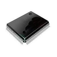
STM32F407VET6 STMicroelectronics, STM32F407VET6 Datasheet - Page 114

STM32F407VET6
Manufacturer Part Number
STM32F407VET6
Description
Microcontrollers (MCU) ARM M4 512 FLASH 168 Mhz 192kB SRAM
Manufacturer
STMicroelectronics
Datasheet
1.STM32F407ZGT6.pdf
(167 pages)
Specifications of STM32F407VET6
Core
ARM Cortex M4
Processor Series
STM32F4
Data Bus Width
32 bit
Maximum Clock Frequency
168 MHz
Program Memory Size
512 KB
Data Ram Size
192 KB
On-chip Adc
Yes
Number Of Programmable I/os
82
Number Of Timers
10
Operating Supply Voltage
1.7 V to 3.6 V
Package / Case
LQFP-100
Mounting Style
SMD/SMT
A/d Bit Size
12 bit
A/d Channels Available
16
Interface Type
CAN, I2C, I2S, SPI, UART
Program Memory Type
Flash
Lead Free Status / Rohs Status
Details
Available stocks
Company
Part Number
Manufacturer
Quantity
Price
Company:
Part Number:
STM32F407VET6
Manufacturer:
ASB
Quantity:
6 700
Company:
Part Number:
STM32F407VET6
Manufacturer:
STMicroelectronics
Quantity:
1
Company:
Part Number:
STM32F407VET6
Manufacturer:
STMicroelectronics
Quantity:
10 000
Part Number:
STM32F407VET6
Manufacturer:
ST
Quantity:
20 000
Company:
Part Number:
STM32F407VET6.
Manufacturer:
ST
Quantity:
15 000
Electrical characteristics
114/167
Figure 42. USB OTG FS timings: definition of data signal rise and fall time
Table 56.
1. Guaranteed by design, not tested in production.
2. Measured from 10% to 90% of the data signal. For more detailed informations, please refer to USB
Table 57.
1. Guaranteed by design, not tested in production.
2. TBD stands for “to be defined”.
f
USB FS interface
Frequency (first transition)
Frequency (steady state) ±500 ppm
Duty cycle (first transition)
Duty cycle (steady state) ±500 ppm
Time to reach the steady state frequency and
duty cycle after the first transition
Clock startup time after the
de-assertion of SuspendM
PHY preparation time after the first transition
of the input clock
HCLK
Symbol
V
Specification - Chapter 7 (version 2.0).
t
CRS
rfm
t
t
r
f
value to guarantee proper operation of
data lines
Differen tial
Rise time
Fall time
Rise/ fall time matching
Output signal crossover voltage
USB OTG FS electrical characteristics
USB FS clock timing parameters
V CRS
Parameter
V S S
(2)
(2)
Parameter
t f
8-bit ±10%
8-bit ±10%
Peripheral
Host
Doc ID 022152 Rev 2
Crossover
points
Driver characteristics
t r
F
F
D
D
T
T
T
T
START_8BIT
STEADY
STEADY
START_DEV
START_HOST
PREP
START_8BIT
STEADY
Symbol
Conditions
C
C
L
L
(1)(2)
-
= 50 pF
= 50 pF
(1)
t
r
/t
f
14.2
TBD
TBD
TBD
TBD
Min
STM32F405xx, STM32F407xx
-
-
-
-
Min
1.3
90
4
4
Nominal
TBD
TBD
TBD
TBD
-
-
-
-
Max
110
2.0
20
20
TBD
TBD
TBD
TBD
TBD
TBD
Max
ai14137
-
-
Unit
ns
ns
%
V
MHz
MHz
MHz
Unit
ms
ms
µs
%
%


