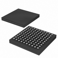
DS3170N+ Maxim Integrated Products, DS3170N+ Datasheet - Page 27

DS3170N+
Manufacturer Part Number
DS3170N+
Description
IC TXRX DS3/E3 100-CSBGA
Manufacturer
Maxim Integrated Products
Datasheet
1.DS3170.pdf
(230 pages)
Specifications of DS3170N+
Function
Single-Chip Transceiver
Interface
DS3, E3
Number Of Circuits
1
Voltage - Supply
3.135 V ~ 3.465 V
Current - Supply
120mA
Operating Temperature
-40°C ~ 85°C
Mounting Type
Surface Mount
Package / Case
100-LBGA
Includes
DS3 Framers, E3 Framers, HDLC Controller, On-Chip BERTs
Lead Free Status / RoHS Status
Lead free / RoHS Compliant
Power (watts)
-
- Current page: 27 of 230
- Download datasheet (3Mb)
8.2 Detailed Pin Descriptions
Table 8-2. Detailed Pin Descriptions
Ipu (input with pullup), Oz (output tri-stateable), Oa (Analog output), Ia (analog input), IO (Bidirectional inout)
UNUSED
TLCLK
TPOS /
TDAT
PIN NAME
UNUSED1
UNUSED2
AVDDC
AVSSR
AVSSC
AVDDJ
AVSST
AVSSJ
NAME
TYPE
O
O
Transmit Line Clock Output
TLCLK: This signal is available when the transmit line interface pins are enabled
(PORT.CR2.
and TNEG signals, but can also be used as the reference for the TSOFI, TSER, and
TSOFO / TDEN signals.
This output signal can be inverted.
o
o
Transmit Positive AMI / Data Output
TPOS: When the port line interface is configured for B3ZS, HDB3 or AMI mode and
the transmit line interface pins are enabled
indicates that a positive pulse should be transmitted on the line. The signal is updated
on the positive clock edge of the referenced clock pin if the clock pin signal is not
inverted, otherwise it is updated on the falling edge of the clock. The signal is typically
referenced to the TLCLK line clock output pins, but it can be referenced to the
TCLKO, TCLKI, RLCLK or RCLKO pins. This output signal can be disabled when the
TX LIU is enabled.
This output signal can be inverted.
TDAT: When the port line interface is configured for UNI mode and the transmit line
interface pins are enabled
output on this pin. The signal is updated on the positive clock edge of the referenced
clock pin if the clock pin signal is not inverted, otherwise it is updated on the falling
edge of the clock. The signal is typically referenced to the TLCLK line clock output
pins, but it can be referenced to the TCLKO, TCLKI, RLCLK or RCLKO pins
This output signal can be inverted.
o
o
DS3: 44.736 MHz +20 ppm
E3: 34.368 MHz +20 ppm
DS3: 44.736 Mbps +20ppm
E3: 34.368 Mbps +20ppm
PIN
G3
G1
G2
D2
D6
E3
B5
E4
TLEN). This clock is typically used as the clock reference for the TDAT
TYPE
PWR
PWR
PWR
PWR
PWR
PWR
N/A
N/A
Analog 3.3V for Jitter Attenuator
Analog 3.3V for CLAD
Analog Ground for Receive LIU
Analog Ground for Transmit LIU
Analog Ground for Jitter Attenuator
Analog Ground for CLAD
Unused
Unused
27 of 230
Line IO
(PORT.CR2.
PIN DESCRIPTION
TLEN), the un-encoded transmit signal is
(PORT.CR2.
DS3170 DS3/E3 Single-Chip Transceiver
FUNCTION
TLEN), a high on this pin
Related parts for DS3170N+
Image
Part Number
Description
Manufacturer
Datasheet
Request
R

Part Number:
Description:
IC TXRX DS3/E3 100-CSBGA
Manufacturer:
Maxim Integrated Products
Datasheet:

Part Number:
Description:
Network Controller & Processor ICs DS3-E3 Single-Chip T ransceiver T3-E3 Fra
Manufacturer:
Maxim Integrated Products
Datasheet:

Part Number:
Description:
MAX7528KCWPMaxim Integrated Products [CMOS Dual 8-Bit Buffered Multiplying DACs]
Manufacturer:
Maxim Integrated Products
Datasheet:

Part Number:
Description:
Single +5V, fully integrated, 1.25Gbps laser diode driver.
Manufacturer:
Maxim Integrated Products
Datasheet:

Part Number:
Description:
Single +5V, fully integrated, 155Mbps laser diode driver.
Manufacturer:
Maxim Integrated Products
Datasheet:

Part Number:
Description:
VRD11/VRD10, K8 Rev F 2/3/4-Phase PWM Controllers with Integrated Dual MOSFET Drivers
Manufacturer:
Maxim Integrated Products
Datasheet:

Part Number:
Description:
Highly Integrated Level 2 SMBus Battery Chargers
Manufacturer:
Maxim Integrated Products
Datasheet:

Part Number:
Description:
Current Monitor and Accumulator with Integrated Sense Resistor; ; Temperature Range: -40°C to +85°C
Manufacturer:
Maxim Integrated Products

Part Number:
Description:
TSSOP 14/A°/RS-485 Transceivers with Integrated 100O/120O Termination Resis
Manufacturer:
Maxim Integrated Products

Part Number:
Description:
TSSOP 14/A°/RS-485 Transceivers with Integrated 100O/120O Termination Resis
Manufacturer:
Maxim Integrated Products

Part Number:
Description:
QFN 16/A°/AC-DC and DC-DC Peak-Current-Mode Converters with Integrated Step
Manufacturer:
Maxim Integrated Products

Part Number:
Description:
TDFN/A/65V, 1A, 600KHZ, SYNCHRONOUS STEP-DOWN REGULATOR WITH INTEGRATED SWI
Manufacturer:
Maxim Integrated Products

Part Number:
Description:
Integrated Temperature Controller f
Manufacturer:
Maxim Integrated Products

Part Number:
Description:
SOT23-6/I°/45MHz to 650MHz, Integrated IF VCOs with Differential Output
Manufacturer:
Maxim Integrated Products

Part Number:
Description:
SOT23-6/I°/45MHz to 650MHz, Integrated IF VCOs with Differential Output
Manufacturer:
Maxim Integrated Products


