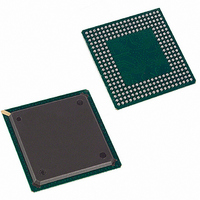
DS21Q55 Maxim Integrated Products, DS21Q55 Datasheet - Page 27

DS21Q55
Manufacturer Part Number
DS21Q55
Description
IC TXRX QUAD T1/E1/J1 SCT 256BGA
Manufacturer
Maxim Integrated Products
Datasheet
1.DS21Q55.pdf
(237 pages)
Specifications of DS21Q55
Function
Transceiver
Interface
E1, J1, T1
Number Of Circuits
4
Voltage - Supply
3.14 V ~ 3.47 V
Current - Supply
75mA
Operating Temperature
0°C ~ 70°C
Mounting Type
Surface Mount
Package / Case
256-BGA
Includes
BERT Generator and Detector, Dual HDLC Controllers
Lead Free Status / RoHS Status
Contains lead / RoHS non-compliant
Power (watts)
-
Available stocks
Company
Part Number
Manufacturer
Quantity
Price
Company:
Part Number:
DS21Q552
Manufacturer:
DALLAS
Quantity:
319
Company:
Part Number:
DS21Q552BN+
Manufacturer:
Maxim Integrated
Quantity:
10 000
Part Number:
DS21Q554
Manufacturer:
DALLAS
Quantity:
20 000
Part Number:
DS21Q554B+
Manufacturer:
MAXIM/美信
Quantity:
20 000
2.5 Line Interface Pins
Signal Name:
Signal Description:
Signal Type:
A (50ppm) clock source is applied at this pin. This clock is used internally for both clock/data recovery
and for the jitter attenuator for T1 and E1 modes. The clock rate can be 16.384MHz, 8.192MHz,
4.096MHz, or 2.048MHz. When using the device in T1-only operation, a 1.544MHz (50ppm) clock
source can be used.
Signal Name:
Signal Description:
Signal Type:
A (50ppm) clock source is applied at this pin. This clock is used internally for both clock/data recovery
and for the jitter attenuator for T1 and E1 modes. The clock rate can be 16.384MHz, 8.192MHz,
4.096MHz, or 2.048MHz. When using the DS21Q55 in T1-only operation, a 1.544MHz (50ppm) clock
source can be used.
Signal Name:
Signal Description:
Signal Type:
Connect low to separate the line interface circuitry from the framer/formatter circuitry and activate the
TPOSI/TNEGI/TCLKI/RPOSI/RNEGI/RCLKI pins. Connect high to connect the line interface circuitry
to the framer/formatter circuitry and deactivate the TPOSI/TNEGI/TCLKI/RPOSI/RNEGI/RCLKI pins.
When LIUC is connected high, the TPOSI/TNEGI/TCLKI/RPOSI/RNEGI/RCLKI pins should be
connected low.
Signal Name:
Signal Description:
Signal Type:
Analog inputs for clock recovery circuitry. These pins connect through a 1:1 transformer to the network.
See Section
Signal Name:
Signal Description:
Signal Type:
Analog line driver outputs. These pins connect through a 1:2 step-up transformer to the network. See
Section
22
for details.
22
for details.
MCLK1
Master Clock Input for Transceivers 1 & 3
Input
MCLK2
Master Clock Input for Transceivers 2 & 4
Input
LIUC
Line Interface Connect
Input
RTIPx and RRINGx
Receive Tip and Ring
Input
TTIPx and TRINGx
Transmit Tip and Ring
Output
27 of 237


