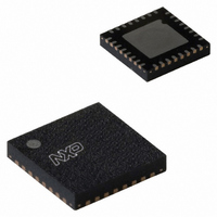
SC16C850SVIBS,157 NXP Semiconductors, SC16C850SVIBS,157 Datasheet - Page 13

SC16C850SVIBS,157
Manufacturer Part Number
SC16C850SVIBS,157
Description
IC UART SGL 1.8V W/FIFO 32-HVQFN
Manufacturer
NXP Semiconductors
Datasheet
1.SC16C850SVIBS151.pdf
(48 pages)
Specifications of SC16C850SVIBS,157
Features
Programmable
Number Of Channels
1, UART
Fifo's
128 Byte
Protocol
RS485
Voltage - Supply
1.8V
With Auto Flow Control
Yes
With Irda Encoder/decoder
Yes
With False Start Bit Detection
Yes
With Modem Control
Yes
With Cmos
Yes
Mounting Type
Surface Mount
Package / Case
32-VFQFN Exposed Pad
Lead Free Status / RoHS Status
Lead free / RoHS Compliant
Other names
935286785157
SC16C850SVIBS
SC16C850SVIBS
SC16C850SVIBS
SC16C850SVIBS
NXP Semiconductors
SC16C850SV
Product data sheet
6.10 Loopback mode
Table 6.
The internal loopback capability allows on-board diagnostics. In the Loopback mode, the
normal modem interface pins are disconnected and reconfigured for loopback internally
(see
In the Loopback mode, the transmitter output (TX) and the receiver input (RX) are
disconnected from their associated interface pins, and instead are connected together
internally. The CTS, DSR, CD, and RI are disconnected from their normal modem control
inputs pins, and instead are connected internally to RTS, DTR, MCR[3] (OP2) and MCR[2]
(OP1). Loopback test data is entered into the transmit holding register via the user data
bus interface, AD[7:0]. The transmit UART serializes the data and passes the serial data
to the receive UART via the internal loopback connection. The receive UART converts the
serial data back into parallel data that is then made available at the user data interface
AD[7:0]. The user optionally compares the received data to the initial transmitted data for
verifying error-free operation of the UART TX/RX circuits.
In this mode, the receiver and transmitter interrupts are fully operational. The modem
control interrupts are also operational.
Output
baud rate
(bit/s)
38.4 k
57.6 k
115.2 k
Figure
Baud rate generator programming table using a 1.8432 MHz clock with
MCR[7] = 0, SAMPR[1:0] = 00b, and CLKPRE[3:0] = 0
6). MCR[3:0] register bits are used for controlling loopback diagnostic testing.
Single UART with 128-byte FIFOs, IrDA, and XScale VLIO bus interface
All information provided in this document is subject to legal disclaimers.
Output
16 clock divisor
(decimal)
3
2
1
Rev. 2 — 22 March 2011
Output
16 clock divisor
(hexadecimal)
03
02
01
DLM
program value
(hexadecimal)
00
00
00
SC16C850SV
…continued
© NXP B.V. 2011. All rights reserved.
DLL
program value
(hexadecimal)
03
02
01
13 of 48


