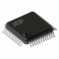
SC16C650BIB48,157 NXP Semiconductors, SC16C650BIB48,157 Datasheet - Page 14

SC16C650BIB48,157
Manufacturer Part Number
SC16C650BIB48,157
Description
IC UART SOT313-2
Manufacturer
NXP Semiconductors
Datasheet
1.SC16C650BIB48151.pdf
(48 pages)
Specifications of SC16C650BIB48,157
Number Of Channels
1, UART
Fifo's
32 Byte
Voltage - Supply
2.5V, 3.3V, 5V
With Auto Flow Control
Yes
With Irda Encoder/decoder
Yes
With False Start Bit Detection
Yes
With Modem Control
Yes
With Cmos
Yes
Mounting Type
Surface Mount
Package / Case
48-LQFP
Lead Free Status / RoHS Status
Lead free / RoHS Compliant
Other names
935274391157
SC16C650BIB48
SC16C650BIB48
SC16C650BIB48
SC16C650BIB48
NXP Semiconductors
SC16C650B_4
Product data sheet
6.10 Loopback mode
6.8 DMA operation
6.9 Sleep mode
The SC16C650B FIFO trigger level provides additional flexibility to the user for block
mode operation. The user can optionally operate the transmit and receive FIFOs in the
DMA mode (FCR[3]). The DMA mode affects the state of the RXRDY and TXRDY output
pins.
Remark: DMA operation is not supported in the HVQFN32 package.
Table 6.
Table 7.
The SC16C650B is designed to operate with low power consumption. A special Sleep
mode is included to further reduce power consumption when the chip is not being used.
With EFR[4] and IER[4] enabled (set to a logic 1), the SC16C650B enters the Sleep
mode, but resumes normal operation when a start bit is detected, a change of state on
any of the modem input pins RI, CTS, DSR, DCD, RX pin, or a transmit data is provided
by the user. If the Sleep mode is enabled and the SC16C650B is awakened by one of the
conditions described above, it will return to the Sleep mode automatically after the last
character is transmitted or read by the user. In any case, the Sleep mode will not be
entered while an interrupt(s) is pending. The SC16C650B will stay in the Sleep mode of
operation until it is disabled by setting IER[4] to a logic 0.
The internal loopback capability allows on-board diagnostics. In the loopback mode, the
normal modem interface pins are disconnected and reconfigured for loopback internally.
MCR[3:0] register bits are used for controlling loopback diagnostic testing. In the loopback
mode, OUT1 (bit 2) and OUT2 (bit 3) in the MCR register control the modem RI and DCD
inputs, respectively. MCR signals DTR (bit 0) and RTS (bit 1) are used to control the
modem DSR and CTS inputs, respectively. The transmitter output (TX) and the receiver
input (RX) are disconnected from their associated interface pins, and instead are
connected together internally (see
disconnected from their normal modem control input pins, and instead are connected
internally to DTR, RTS, OUT1 and OUT2. Loopback test data is entered into the Transmit
Holding Register via the user data bus interface, D0 to D7. The transmit UART serializes
the data and passes the serial data to the receive UART via the internal loopback
connection. The receive UART converts the serial data back into parallel data that is then
made available at the user data interface D0 to D7. The user optionally compares the
received data to the initial transmitted data for verifying error-free operation of the UART
TX/RX circuits.
Non-DMA mode
1 = FIFO empty
0 = at least 1 byte in FIFO
Non-DMA mode
1 = at least 1 byte in FIFO
0 = FIFO empty
Table 6
Effect of DMA mode on state of RXRDY pin
Effect of DMA mode on state of TXRDY pin
and
Table 7
Rev. 04 — 14 September 2009
show this.
DMA mode
0-to-1 transition when FIFO empties
1-to-0 transition when FIFO reaches trigger level, or time-out occurs
DMA mode
0-to-1 transition when FIFO becomes full
1-to-0 transition when FIFO has 1 empty space
UART with 32-byte FIFOs and IrDA encoder/decoder
Figure
7). The CTS, DSR, DCD, and RI are
SC16C650B
© NXP B.V. 2009. All rights reserved.
14 of 48


