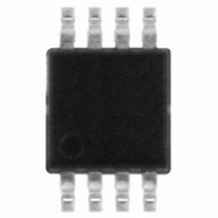
TS421IST STMicroelectronics, TS421IST Datasheet - Page 28

TS421IST
Manufacturer Part Number
TS421IST
Description
IC AMP AUDIO PWR .367W AB 8MSOP
Manufacturer
STMicroelectronics
Type
Class ABr
Datasheet
1.TS419IDT.pdf
(32 pages)
Specifications of TS421IST
Output Type
1-Channel (Mono)
Max Output Power X Channels @ Load
367mW x 1 @ 16 Ohm
Voltage - Supply
2 V ~ 5.5 V
Features
Differential Inputs, Short-Circuit Protection, Standby
Mounting Type
Surface Mount
Package / Case
8-MSOP, Micro8™, 8-uMAX, 8-uSOP,
Lead Free Status / RoHS Status
Lead free / RoHS Compliant
Other names
497-4449-2
TS419-TS421
The efficiency is the ratio between the output
power and the power supply
The maximum theoretical value is reached when
Vpeak = Vcc, so
Two capacitors are needed to bypass properly the
TS419/TS421. A power supply bypass capacitor
C
C
high frequency region (above 7kHz) and an
indirect influence on power supply disturbances.
With 1µF, you can expect similar THD+N
performances to those shown in the datasheet.
In the high frequency region, if C
1µF, it increases THD+N and disturbances on the
power supply rail are less filtered.
On the other hand, if C
disturbances on the power supply rail are more
filtered.
C
frequencies, but its function is critical to the final
result of PSRR (with input grounded and in the
lower frequency region).
If C
frequencies and PSRR worsens.
If C
lower frequencies is small, but the benefit to PSRR
is substantial.
Note that C
at lower frequencies. The lower the value of C
the higher the PSRR.
When standby is released to put the device ON,
the bypass capacitor C
immediatly. As C
the amplifier, the bias will not work properly until
the C
voltage is called wake-up time or T
equal to:
T
28/32
WU
S
S
B
Decoupling of the circuit
Wake-up Time: T
and a bias voltage bypass capacitor C
B
B
has particular influence on the THD+N in the
=0.15xC
has an influence on THD+N at lower
is lower than 1µF, THD+N increases at lower
B
is higher than 1µF, the benefit on THD+N at
voltage is correct. The time to reach this
IN
B
has a non-negligible effect on PSRR
(s) with C
B
P
is directly linked to the bias of
P
sup
4
OUT
WU
ply
S
B
78
B
will not be charged
is higher than 1µF, those
in µF.
5 .
%
4
V
Vcc
PEAK
WU
S
is lower than
and typically
B
.
IN
,
Due to process tolerances, the range of the
wake-up time is :
0.12xCb < T
Note : When the standby command is set, the time
to put the device in shutdown mode is a few
microseconds.
Pop performance is intimately linked with the size
of the input capacitor Cin and the bias voltage
bypass capacitor C
The size of C
frequency and PSRR values requested. The size
of C
requested at lower frequencies.
Moreover, C
amplifier turns ON. The slower the speed is, the
softer the turn ON noise is.
The charge time of C
the internal generator resistance 150k ..
Then, the charge time constant for C
As C
input (pin 2 & 3) and if we want to minimize, in
amplitude and duration, the output spike on Vout1
(pin 5), C
equivalent charge time constant of C
Thus we have the relation:
Proper respect of this relation allows to minimize
the pop noise.
Remark : Minimizing C
pop phenomena, and the cost and size of the
application.
The schematic on figure 98, shows how to design
the TS419/21 to work in a differential input mode.
The gain of the amplifier is:
In order to reach optimal
performances of the differential function, R
R
B
IN
IN
2
Pop performance
Application : Differential inputs BTL power
amplifier.
= 150k xC
should be matched at 1% max.
= (Rin+Rfeed)xC
<
B
B
is dependent on THD+N and PSRR values
B
is directly connected to the non-inverting
IN
(s)
B
must be charged faster than C
WU
IN
determines the speed with which the
B
< 0.18xC
is dependent on the lower cut-off
(s)
B
.
IN
B
IN
(s)
is directly proportional to
B
and C
(s) with C
B
G
benefits both the
VDIFF
B
B
IN
in µF
is
is:
2
1
B
and
. The
R
R
2
1


